

-
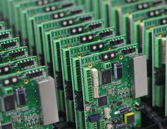
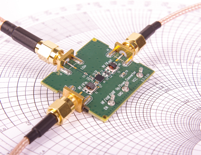
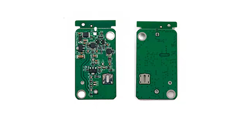
Products -PCBA Manufacturing RF Connectors RF Cable Assemblys Embedded Antennas External Antennas Positioning Chips and Modules
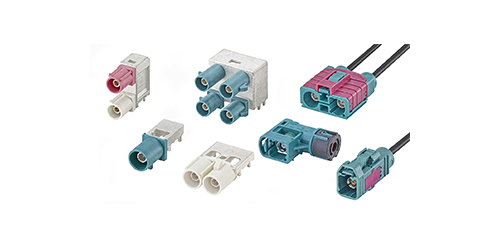
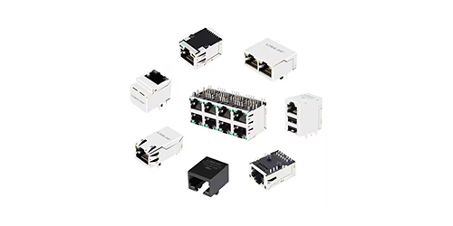
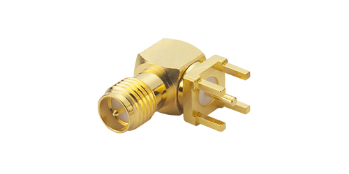
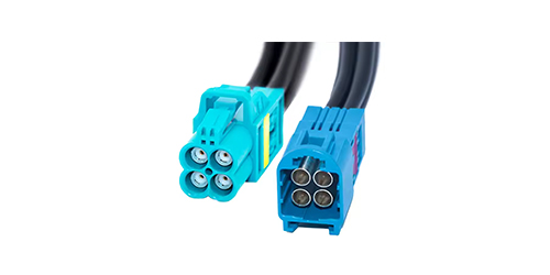
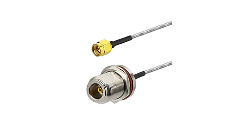
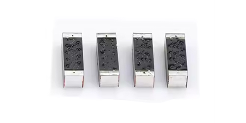
RF Connectors

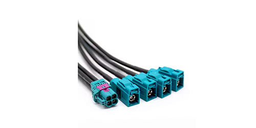
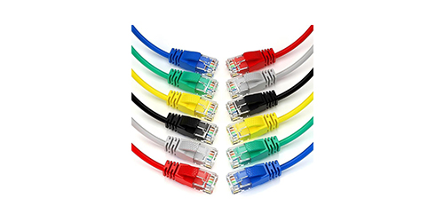
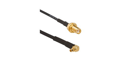
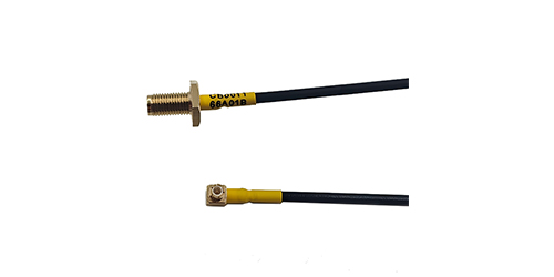
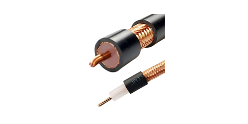
RF Cable Assemblys
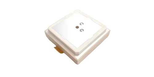
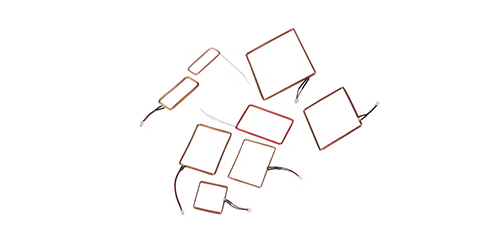
Embedded Antennas
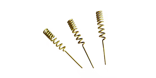
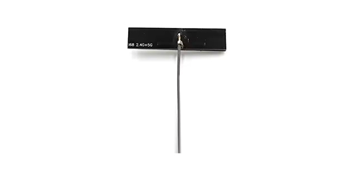
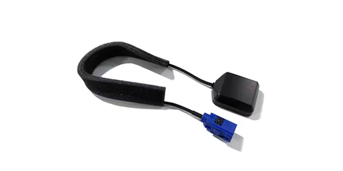
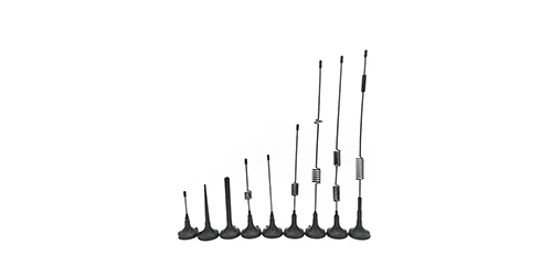
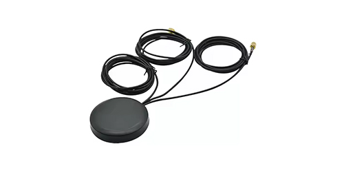
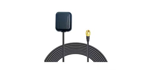
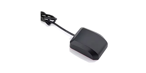
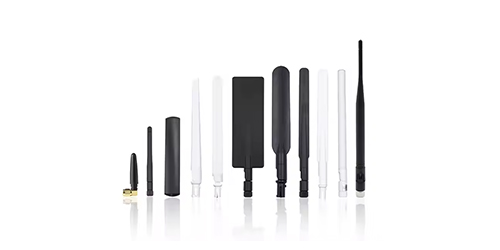
External Antennas
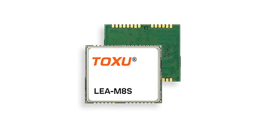
Positioning Chips and Modules
 Language


Language

The Internet of Things (IoT) represents a fundamental shift in how we interact with the physical world, envisioning a global network of interconnected devices—from city infrastructure and industrial machinery to household appliances and personal wearables—constantly sensing, communicating, and acting upon data. For a vast number of these applications, a critical piece of information is context: Where is the device? Where has it been? Is it moving? This contextual layer of location intelligence transforms a simple sensor node into a smart, spatially-aware entity, enabling applications that were previously impossible or impractical.
The Internet of Things (IoT) represents a fundamental shift in how we interact with the physical world, envisioning a global network of interconnected devices—from city infrastructure and industrial machinery to household appliances and personal wearables—constantly sensing, communicating, and acting upon data. For a vast number of these applications, a critical piece of information is context: Where is the device? Where has it been? Is it moving? This contextual layer of location intelligence transforms a simple sensor node into a smart, spatially-aware entity, enabling applications that were previously impossible or impractical.
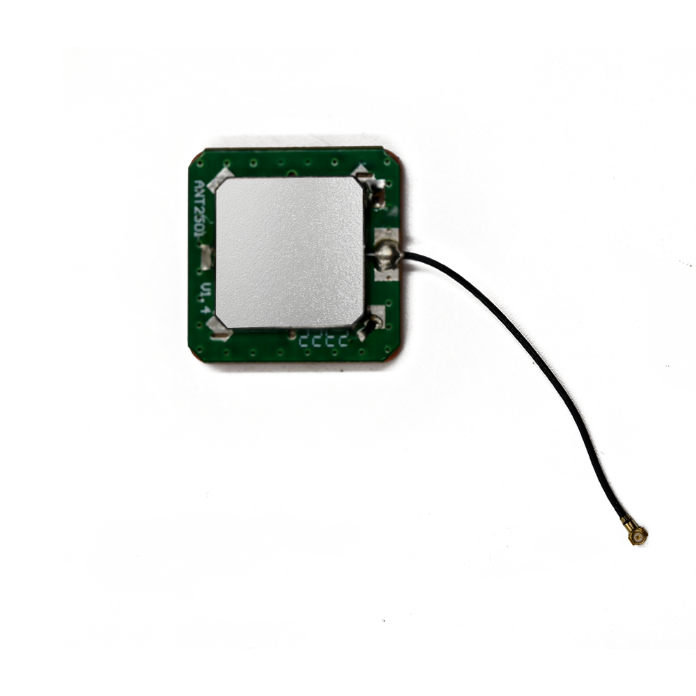
At the core of providing this absolute outdoor positioning capability for IoT is the Global Positioning System (GPS) and other Global Navigation Satellite Systems (GNSS). However, integrating satellite navigation into an IoT device presents a unique set of extreme constraints: ultra-low power consumption, minimal cost, tiny form factors, and the need for robust, set-and-forget operation. The built-in GPS ceramic antenna is the technological component specifically engineered to meet these challenges, acting as the essential gateway between the device and the satellite constellations orbiting above.
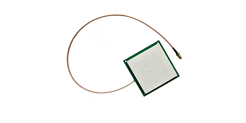
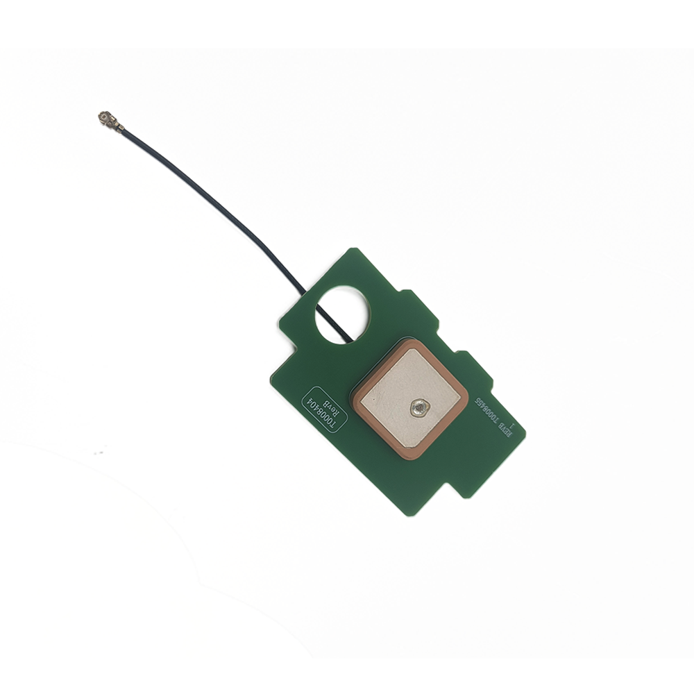
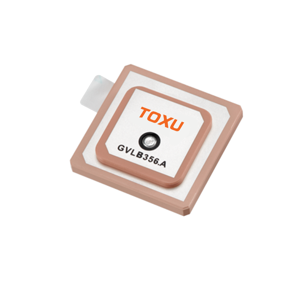
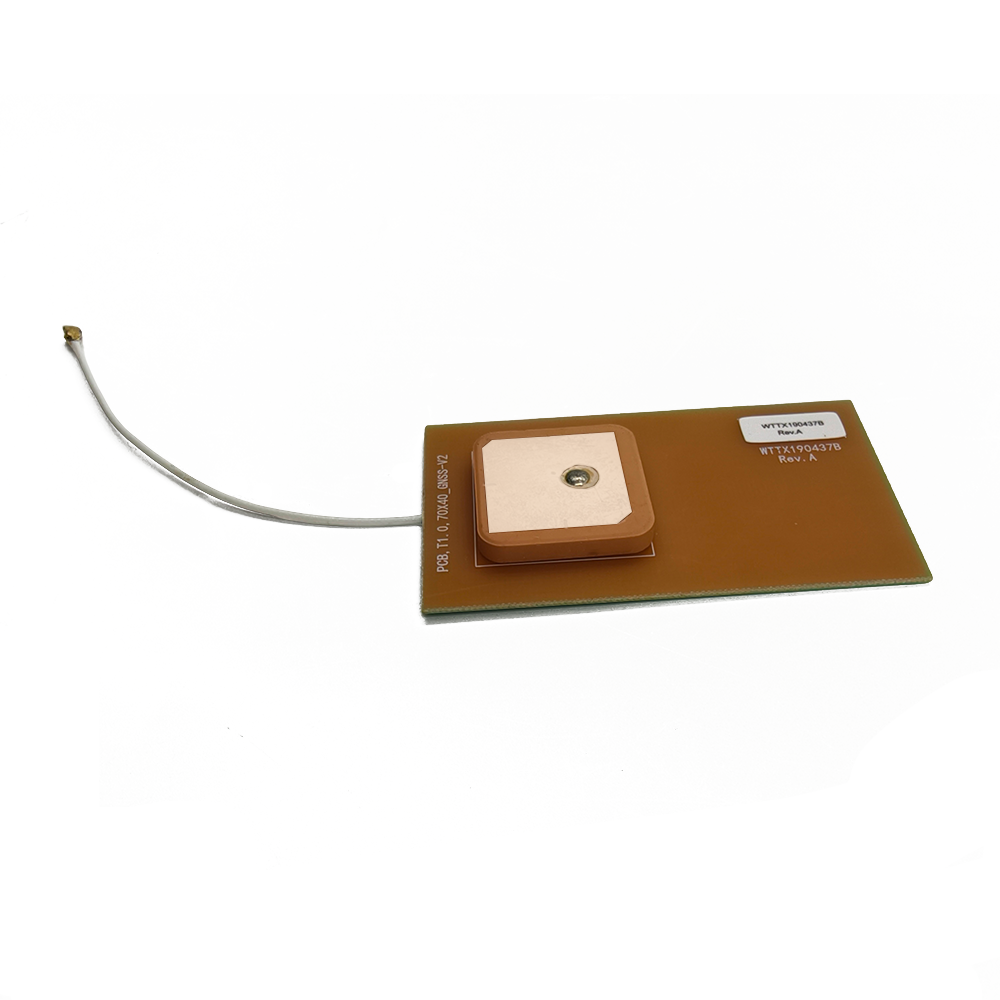
A built-in GPS ceramic antenna for IoT is a type of passive microstrip antenna designed to be directly mounted onto a device's printed circuit board (PCB). Unlike external active antennas with integrated Low-Noise Amplifiers (LNAs) and separate cabling, this antenna is a fundamental part of the device's PCB architecture. Its primary role is to efficiently capture the incredibly weak L-band radio signals (around 1.575 GHz for GPS L1) transmitted by GNSS satellites and convert them into conducted electrical signals that can be processed by a GNSS receiver chip.
The driving philosophy behind these antennas is integration and miniaturization. The high dielectric constant (εr) of ceramic materials—typically between 20 and 40—allows the antenna's physical dimensions to be shrunk dramatically while maintaining the correct electrical resonant length. This makes ceramic patches the ideal technology for embedding into the increasingly compact housings of modern IoT devices, such as asset trackers, wearable health monitors, and agricultural sensors.
Furthermore, the "built-in" nature is crucial for reliability and cost. Eliminating external cables, connectors, and separate antenna housings reduces the Bill of Materials (BOM) cost, simplifies the assembly process, and removes common points of failure like cable wear-and-tear and connector corrosion. This results in a more robust and maintenance-free product, which is a paramount requirement for IoT deployments that may involve thousands of devices deployed in hard-to-reach locations for years at a time.
However, this high level of integration comes with significant engineering challenges. The performance of a built-in antenna is intrinsically linked to the design of the host PCB, the placement of other components, and the material of the device's enclosure. Unlike an external antenna with a defined ground plane and isolation, a built-in antenna's performance can be severely degraded by nearby noise-emitting circuits, the absence of a sufficient ground plane, or a metallic housing that blocks RF signals.
In essence, the built-in GPS ceramic antenna is a masterpiece of compromise. It sacrifices the ultimate performance of a larger, external survey-grade antenna for the supreme advantages of miniaturization, cost-effectiveness, and ruggedness. It is the silent, unassuming sentinel that allows a tiny, battery-powered device to know its place on the globe, enabling the vast, location-aware network that defines the IoT revolution. This overview sets the stage for understanding the delicate balance of design, physics, and practical integration that allows this component to function effectively.
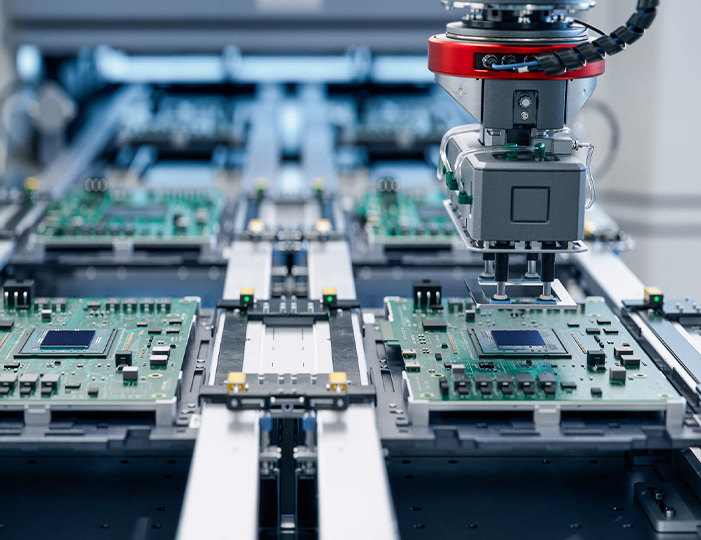
The design and construction of a built-in GPS ceramic antenna for IoT is a meticulous process that balances electromagnetic performance with the harsh realities of mass production and integration. Every aspect, from material selection to physical dimensions, is optimized for its specific role within a constrained environment.
1. Ceramic Substrate: The Foundation
The choice of ceramic material is the most critical decision, defining the antenna's size, efficiency, and bandwidth.
Material Composition: High-purity, fine-grained ceramics are used, typically based on aluminum oxide (Alumina, Al₂O₃) or more advanced titanium-based compounds. These are chosen for their excellent high-frequency properties.
Dielectric Constant (εr): Ranges from ~20 to 40. A higher εr allows for a smaller physical size (as size is inversely proportional to √εr) but comes at the cost of reduced bandwidth and potentially lower radiation efficiency due to increased field concentration within the material itself. For IoT devices, where size is paramount, ceramics with εr > 30 are common.
Loss Tangent (tan δ): This must be exceptionally low (e.g., < 0.002) to minimize dielectric losses. Any energy converted to heat within the ceramic is energy not radiated or received, directly impacting the system's sensitivity and time-to-first-fix (TTFF).
Temperature Stability: The ceramic's properties must remain stable over the device's operational temperature range (often -40°C to +85°C). Thermal expansion or changes in εr can detune the antenna, shifting its resonant frequency.
2. Radiating Patch and Feed Structure
Patch Element: A thin layer of highly conductive material (usually silver or gold applied via thick-film printing or plating) forms the radiating element on the top surface of the ceramic. Its length (L) is designed to be approximately half the wavelength within the dielectric (λ₀ / (2√εr)) to achieve resonance at the target frequency (e.g., 1575.42 MHz for GPS L1).
Feeding Mechanism: How power is transferred to/from the patch is vital for impedance matching (to 50 Ω).
Probe Feed: A common method where a pin is soldered to the patch and passes through a via hole to the feed point on the PCB. It's robust but can introduce parasitic inductance.
Coaxial Feed: The ceramic antenna is manufactured with a pre-attached miniature coaxial cable and connector, which is then soldered to the PCB. This offers good performance but is less ideal for fully automated SMT assembly.
Ceramic SMD Antennas: The most integrated solution. The antenna is a surface-mount device (SMD) with contact pads on its bottom side. It is fed by a microstrip line on the host PCB that runs directly to these pads. This is the cheapest and most automatable solution but requires extremely careful PCB layout.
A patch antenna is a resonant structure that requires a ground plane to function correctly. For a built-in antenna, this ground plane is not part of the antenna component itself but is a dedicated section of the host device's PCB.
Size and Shape: The ground plane is a critical part of the antenna system. Its size and shape significantly influence the antenna's radiation pattern, gain, and bandwidth. A typical rule of thumb is that the PCB ground plane should extend at least a quarter-wavelength (~4-5 cm at GPS L1) beyond the edges of the ceramic patch for optimal performance. This is often a major constraint in tiny IoT devices.
Clearance Zone: The area directly underneath and immediately surrounding the antenna must be kept completely free of other components and copper pours (except for its own feedline). Any metal in this "keep-out" area will capacitively couple to the antenna, detuning it and reducing efficiency.
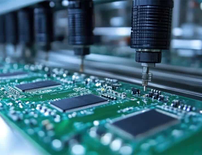
4. Construction and Assembly
Monolithic Design: The ceramic block, radiating patch, and often a protective coating are sintered or fused into a single, robust component.
Mounting: SMD-type antennas are picked and placed by automated machinery and run through a reflow soldering oven alongside all other components, minimizing assembly cost.
Housing Considerations: The device's plastic enclosure acts as the antenna's radome. The plastic material must be RF-transparent (low dielectric constant and loss tangent). Common choices include ABS, PC, and PP. The distance between the antenna and the housing must be carefully controlled, as nearby plastic (with a εr > 1) can load the antenna, lowering its resonant frequency.
The construction of the antenna itself is only half the battle. Its performance is utterly dependent on a correct PCB layout designed in tandem with the antenna's specifications. A perfect antenna can be rendered useless by a poor ground plane or noisy neighboring components, making the design a co-dependent exercise between the antenna manufacturer and the IoT product designer.
The operation of a built-in ceramic patch antenna is a practical application of fundamental electromagnetic theory, tailored to receive signals of extraordinary weakness.
Fundamental Resonance:
The patch antenna operates as a half-wavelength resonant cavity. The ceramic substrate forms the dielectric medium, bounded on top by the conductive patch and on the bottom by the system's ground plane. The antenna is designed to excite the fundamental TM₁₀ mode. At this mode, the length L of the patch determines the resonant frequency, approximately given by:
L ≈ λ₀ / (2 * √εr)
where λ₀ is the free-space wavelength (~19 cm for GPS L1) and εr is the dielectric constant of the ceramic. For εr = 36, L becomes about 1.58 cm, demonstrating the miniaturization effect.
Radiation Mechanism:
The radiation does not come from the patch itself but from the fringing fields at its edges. The electric field lines fringe out between the radiating edge of the patch and the ground plane, creating an effective radiating slot. For a rectangular patch, the two ends along the length L are the primary radiators. Their radiation combines to form a broad, directional pattern perpendicular to the plane of the antenna, which is ideal for receiving signals from satellites overhead.
Polarization:
GNSS satellites transmit Right-Hand Circularly Polarized (RHCP) signals. A simple patch antenna is linearly polarized. To achieve circular polarization, the antenna must excite two orthogonal modes with equal amplitude and a 90-degree phase difference. For IoT ceramic patches, this is most commonly achieved through a single-feed design with a physical perturbation. A common technique is to truncate two opposite corners of the square patch or to add a small tab. This unbalances the two fundamental modes, creating the required phase shift and converting the antenna's polarization to RHCP. This is crucial for rejecting reflected signals (which often reverse to LHCP) and for maintaining consistent signal strength regardless of the satellite's orientation relative to the device.
The Role of the Ground Plane:
The ground plane is not passive; it is an active part of the antenna system. It serves two key functions:
It creates the directional pattern, providing gain towards the sky and attenuating signals coming from below the horizon (which are often noise or multipath reflections).
It acts as an electrical mirror, defining the antenna's impedance and radiation properties. The size of the ground plane directly affects the antenna's performance. A ground plane that is too small can lead to a distorted pattern, reduced gain, and a shift in the antenna's resonant frequency.
The Challenge of Weak Signals:
GPS signals are incredibly weak by the time they travel over 20,000 km to Earth's surface, with a received power level often below -130 dBm—significantly weaker than the thermal noise floor of the receiver. The antenna's job is to capture this faint energy as efficiently as possible. Any loss in the system—due to inefficient radiation, impedance mismatch, or absorption by nearby materials—directly reduces the signal-to-noise ratio (SNR). A drop in SNR translates to longer time-to-first-fix (TTFF), poorer accuracy, and a higher likelihood of losing satellite lock, especially in challenging environments like urban canyons or under foliage. For an IoT device, this can mean failed data reports and depleted batteries as the receiver struggles longer to get a fix.
Therefore, the working principle is not just about resonance; it's about maximizing the efficiency of capturing and delivering these whisper-like signals to the receiver with minimal degradation, all within the confines of a small, noisy, and crowded electronic device.
Applications:
Built-in GPS ceramic antennas are the enabling technology for a vast array of IoT applications:
Asset Tracking: Monitoring the location of shipping containers, pallets, vehicles, and high-value equipment globally.
Fleet Management: Providing location data for logistics and transportation vehicles.
Wearables: Powering location features in fitness trackers, smartwatches, and personal safety devices.
Smart Agriculture: Enabling field mapping, asset tracking, and monitoring of environmental conditions with geotagging.
Industrial IoT (IIoT): Tracking tools, machinery, and personnel within large industrial facilities and construction sites.
Smart City Infrastructure: Monitoring the status and location of infrastructure like smart bins, lighting, and sensors.
Future Trends:
Multi-Band / Wideband Designs: As IoT demands higher accuracy and robustness, antennas that can receive signals from multiple constellations (GPS, Galileo, etc.) and multiple frequencies (L1, L5, L2) will become more common, requiring more advanced ceramic designs.
Hybrid Positioning Antennas: Single antenna components that integrate elements for GPS, Wi-Fi, Bluetooth, and even cellular (4G/5G) into a single package to support hybrid location technologies.
AI-Enhanced RF Design: Using machine learning algorithms to optimize antenna geometry and PCB layout for performance, speeding up the design process and overcoming complex environmental interactions.
"Antenna-on-Chip" and "Antenna-in-Package": Further integration where the antenna is fabricated directly onto the module's substrate or even integrated into the IC package itself, reducing size and cost even further.
Enhanced Resilience to Interference: Designs that are more immune to noise from the host device and jamming/spoofing from the external environment.
Conclusion
The built-in GPS ceramic antenna is a quintessential enabling technology for the Internet of Things. It embodies the core IoT principles of miniaturization, cost reduction, and integration, allowing virtually any device to gain awareness of its geographical location. While it represents a performance compromise compared to larger external antennas, its advantages in size, cost, and ruggedness make it the only practical choice for the vast majority of mass-deployed IoT applications.
Its successful implementation is a testament to sophisticated RF engineering, requiring a deep understanding of the complex interplay between a miniature ceramic component and the device it resides within. As IoT continues to evolve, pushing towards greater accuracy, lower power, and smaller form factors, the built-in ceramic antenna will continue to advance, remaining the silent, indispensable sentinel that connects the physical world of things to the digital world of data.

 86 0755 2819 9597
Lucy Yang | lucy.y@toxutech.com
Nicole Li | nicole@toxutech.com
Dotty Zhao | sales04@toxutech.com
Global Business Director / Sales Team / Global Operations


 En
En Cn
Cn Korean
 Home >


