

-
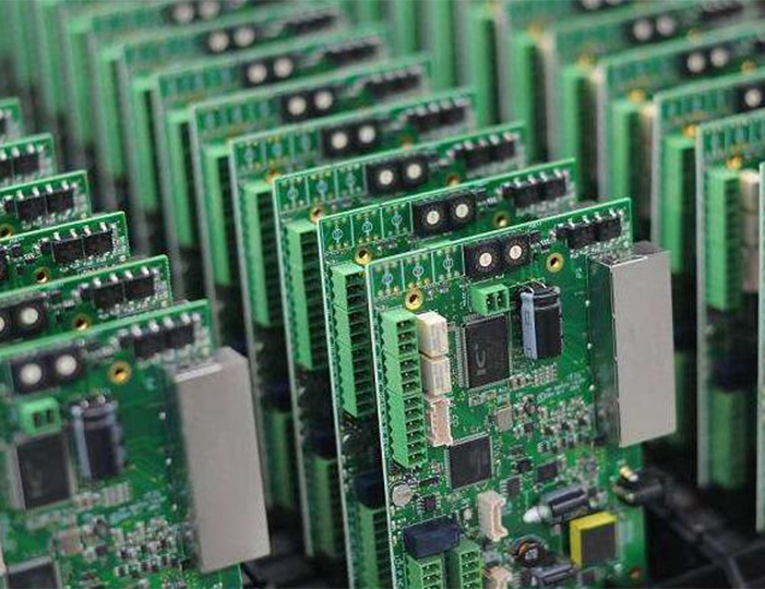
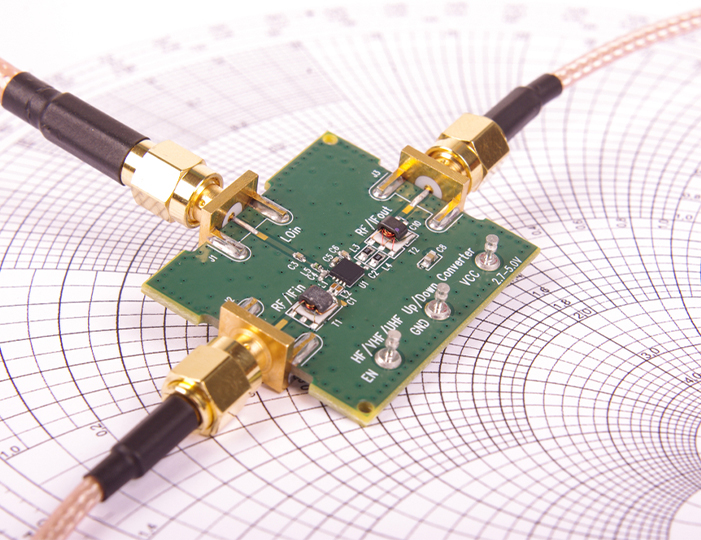
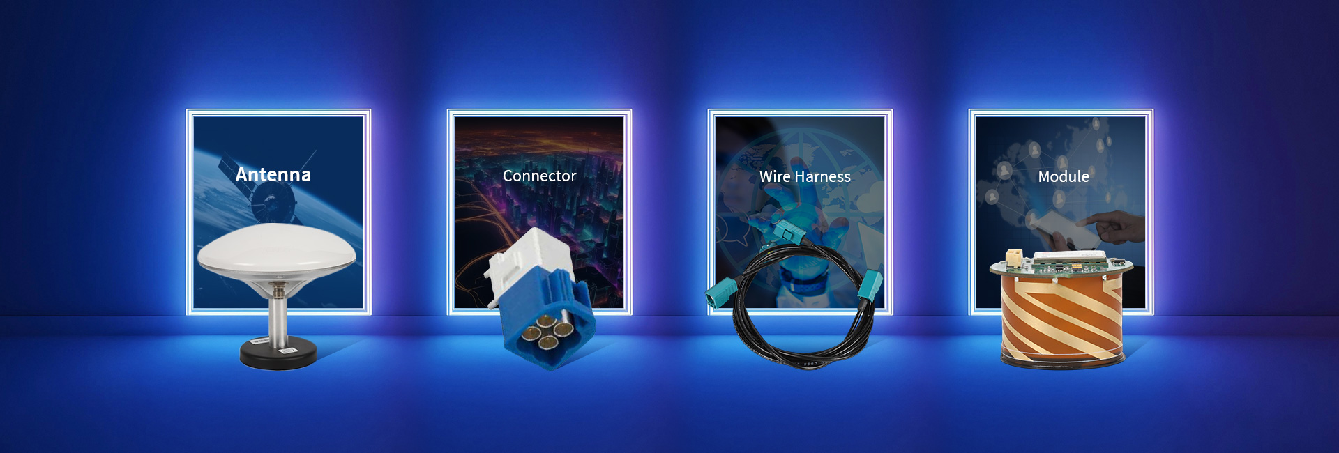
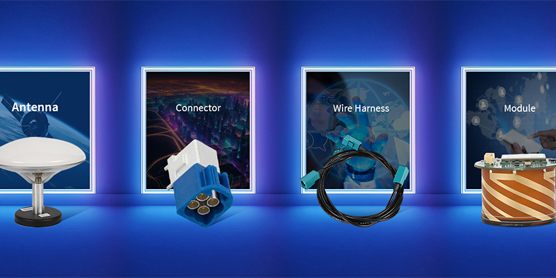
Products -PCBA Manufacturing RF Connectors RF Cable Assemblys Embedded Antennas External Antennas Positioning Chips and Modules
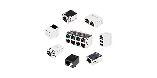
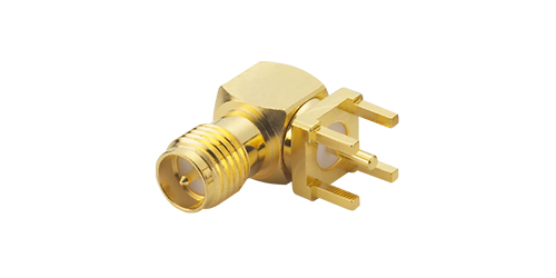
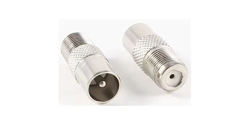
RF Connectors

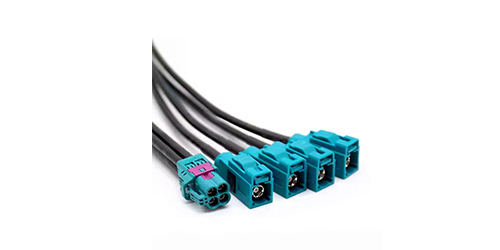
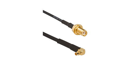
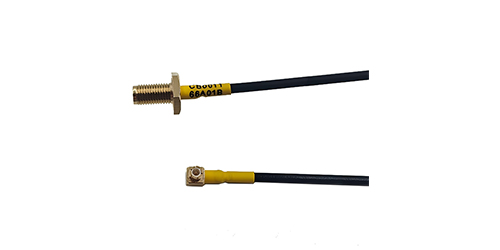
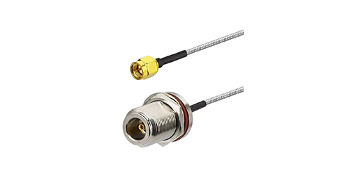
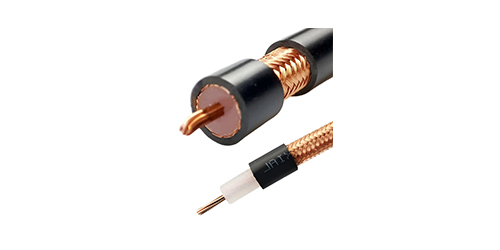
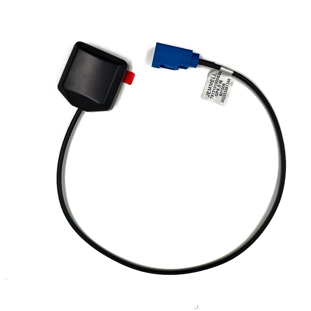
RF Cable Assemblys
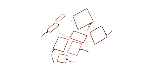
Embedded Antennas
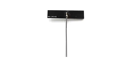
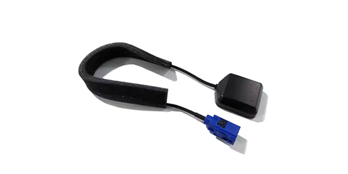
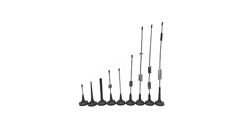
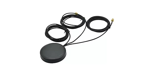
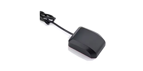
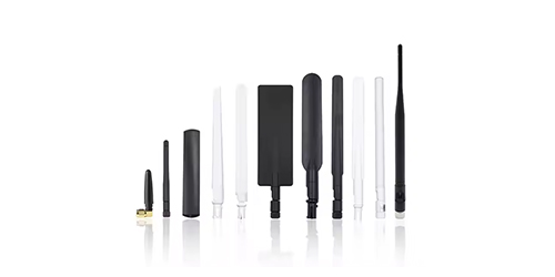
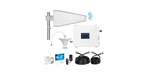
External Antennas
Positioning Chips and Modules
 Language


Language

In the relentless pursuit of miniaturization and seamless integration that defines modern electronics, the antenna has often been a stubborn obstacle. Traditional whip and external antennas disrupt sleek product designs, consume valuable space, and are vulnerable to damage. The ultra-thin low-profile ceramic antenna represents a revolutionary solution to this challenge, embodying the convergence of materials science, electromagnetic engineering, and industrial design. It is a component engineered not just for performance, but for invisibility, enabling the wireless connectivity that is fundamental to contemporary devices without compromising their form factor.
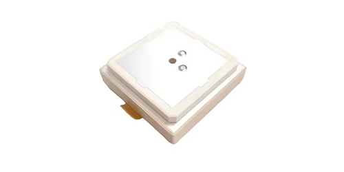
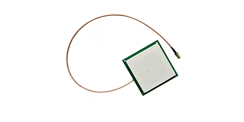
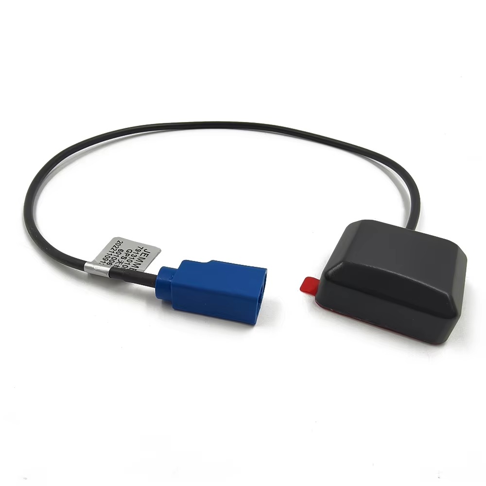
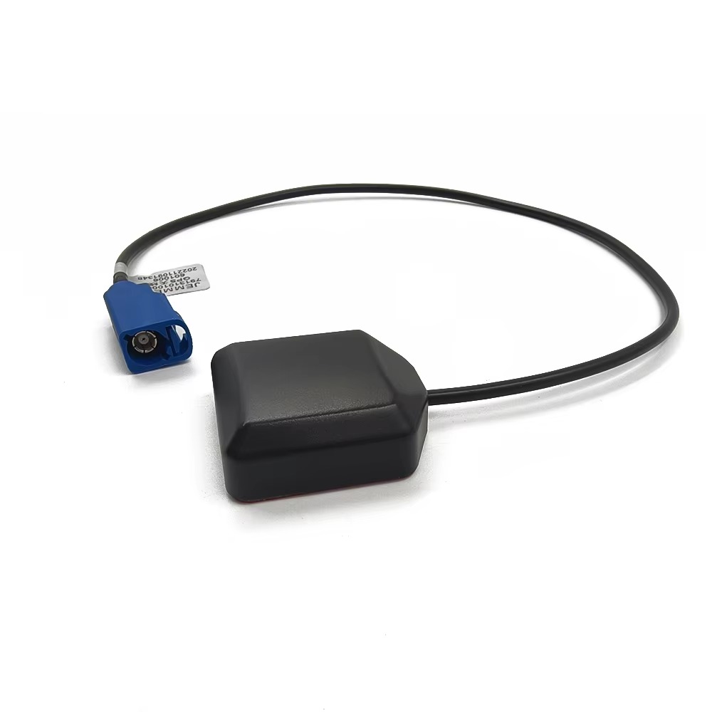
An ultra-thin low-profile ceramic antenna is a type of internal patch antenna specifically designed to be embedded within electronic devices. The term "ultra-thin" and "low-profile" typically describe antennas with a height (z-axis) of less than 2 millimeters, and often as slim as 0.8mm or even 0.5mm. This is a remarkable feat, considering it must efficiently radiate electromagnetic waves at microwave frequencies, such as the 2.4 GHz and 5 GHz bands for Wi-Fi and Bluetooth, or the 1575.42 MHz GPS L1 band. The key enabling technology is the use of a ceramic substrate with a very high dielectric constant (εr), which allows the antenna's physical dimensions to be dramatically reduced while maintaining its electrical resonance.
The primary role of this antenna is to serve as the critical interface between the device's internal circuitry and the external wireless world. In a smartphone, it might handle Wi-Fi, Bluetooth, and GNSS reception. In a wearable fitness tracker, it enables Bluetooth connectivity to a phone. In an IoT sensor, it might provide a cellular LTE-M connection. Its mission is to do this reliably while conforming to the severe spatial constraints imposed by the device's industrial design. These antennas are almost always passive components, meaning they rely on the device's own transmitter power and receiver sensitivity, making their efficiency and integration absolutely paramount.
The driving force behind the development of these antennas is the consumer electronics market's demand for thinner, lighter, and more aesthetically pleasing devices. A protruding antenna is no longer acceptable. Furthermore, the explosion of the Internet of Things (IoT) has created a need for wireless connectivity in incredibly compact form factors—from credit-card-sized asset trackers to miniature medical implants—where a traditional antenna is simply not an option. The ceramic antenna's surface-mount technology (SMT) compatibility makes it ideal for high-volume, automated PCB assembly, further accelerating its adoption.
However, this miniaturization comes with significant engineering challenges. A smaller antenna typically has narrower bandwidth and lower efficiency compared to its larger counterparts. The ultra-thin profile makes its performance exquisitely sensitive to its immediate environment—the proximity of the device's battery, display, metal casing, and even the user's hand can detune its resonant frequency and drastically reduce its effectiveness. Therefore, designing with these antennas is not a simple component selection; it is a complex process of co-design, where the antenna, the PCB layout, and the device's housing are all optimized together.
In essence, the ultra-thin low-profile ceramic antenna is a masterpiece of compromise and innovation. It willingly trades some degree of raw performance for the unparalleled advantage of near-invisibility. It is the unsung enabler of the wireless revolution, hiding in plain sight within our most cherished gadgets, allowing them to connect to the digital world without betraying their sleek, minimalist exteriors. It is the definitive answer to the question of how to build wireless functionality into devices that are increasingly defined by their lack of free space.
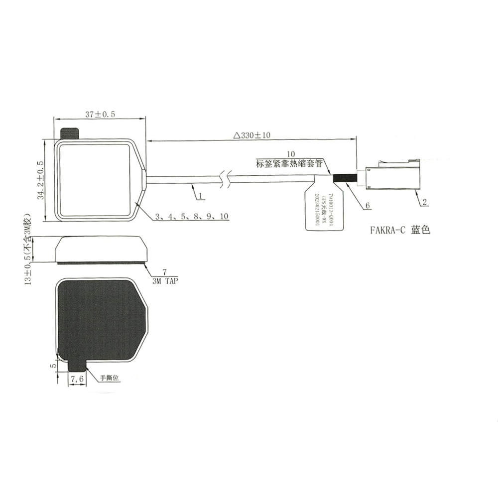
The design and construction of an ultra-thin low-profile ceramic antenna is a meticulous process that balances electromagnetic physics with the harsh realities of mass manufacturing and miniaturization. It is a multi-layered structure where every micron of material and every millimeter of trace length is calculated to achieve target performance within an extraordinarily constrained volume.
1. The Ceramic Substrate: The Engine of Miniaturization
The foundation of the antenna is a specially formulated ceramic slab. This is not a standard ceramic but a proprietary composite, often based on titanium-based ceramics or other complex oxides, engineered for specific properties:
Very High Dielectric Constant (εr): This is the most critical parameter. Values typically range from 20 to over 80. A high εr (e.g., 40) reduces the wavelength within the material by a factor of √40 ≈ 6.3. This allows the physical length of the radiating patch to be correspondingly smaller to resonate at the same frequency, enabling the ultra-thin form factor.
Extremely Low Loss Tangent (tan δ): Despite the high εr, the material must have minimal electromagnetic loss (tan δ < 0.002 is common). A high loss tangent would cause the antenna to dissipate transmitted power as heat within the ceramic itself, drastically reducing its radiation efficiency and range.
Temperature Stability: The dielectric constant must remain stable over the device's operating temperature range (e.g., -30°C to +85°C). Thermal drift would shift the antenna's resonant frequency, potentially moving it outside the desired communication band.
2. The Radiating Element: The Patch
A conductive radiating patch is fabricated on the top surface of the ceramic block. This is typically achieved through a process like screen printing a silver-based conductive paste onto the raw ceramic, which is then co-fired in a high-temperature kiln. This fuses the metal to the substrate, creating a durable and low-resistance layer.
Patch Geometry: The patch is most commonly rectangular or square. Its length L is the primary determinant of the resonant frequency and is calculated to be slightly less than half the wavelength within the dielectric material (λ_d/2) at the target frequency.
Multi-Band Designs: To cover multiple bands (e.g., 2.4 GHz and 5 GHz for Wi-Fi), more complex designs are used. These can include:
Stacked Patches: A second, smaller parasitic patch on a separate ceramic layer is placed above the primary patch for the higher frequency.
Slotted Patches: Inserting slots of specific shapes and sizes into the patch can perturb the current distribution and create multiple resonant paths.
Multiple Feed Points: Using separate feed points for different frequencies on a single, specially shaped patch.
3. The Feed Mechanism: Delivering the Signal
The antenna must be connected to the device's RF transceiver. The two main techniques are:
Probe Feeding: A small pin (probe) is soldered to the patch and passes through a hole drilled in the ceramic to connect to a microstrip feedline on the bottom of the PCB. This is a common and robust method.
Aperture-Coupled Feeding: A more advanced technique where the patch is on the top layer. Energy is coupled from a microstrip feedline on the host PCB through a slot etched in an intermediate ground plane. This offers better bandwidth and isolation but is more complex.
4. The Ground Plane: A Critical External Dependency
Unlike larger antennas, the ultra-thin ceramic patch antenna does not typically include its own ground plane. Instead, it is critically dependent on the ground plane of the host printed circuit board (PCB). This ground plane, which must be provided in the device's design, serves as the electrical counterpoise for the antenna. Its size, shape, and proximity are fundamental to the antenna's performance, influencing its bandwidth, efficiency, and radiation pattern. The absence of an adequate ground plane will render the antenna useless.
5. Achieving Miniaturization and Challenges
The extreme thinness is achieved by using ceramics with the highest possible dielectric constants. However, this comes with a fundamental trade-off: Bandwidth.
The bandwidth of a patch antenna is inversely proportional to both the electrical volume it occupies and the dielectric constant of the substrate. A high εr allows for a small physical size but also results in a very small electrical size, which inherently narrows the operational bandwidth. This is the primary design challenge: achieving a bandwidth wide enough to cover the desired frequency band (e.g., the 100 MHz required for Wi-Fi 2.4 GHz) with a material that is trying to make it narrow.
6. Final Assembly and Packaging
The final antenna component is a single, monolithic ceramic block with metallization. It is designed as a surface-mount device (SMD), with solderable terminals on its bottom side. This allows it to be automatically picked and placed by assembly robots and soldered onto the PCB in a reflow oven alongside resistors and capacitors, making it ideal for high-volume production. The entire component is robust, resistant to mechanical shock, and ready to be integrated into the final product.
The operation of an ultra-thin low-profile ceramic antenna is a practical application of resonant cavity theory, pushed to the limits of miniaturization. Its working principle revolves around creating and radiating a standing wave within a drastically reduced physical space, a task that requires careful management of inherent trade-offs and a deep understanding of its interaction with the host device.
Fundamental Resonance in a Miniaturized Cavity
At its core, the antenna functions as a resonant cavity. The top metallized patch and the ground plane on the host PCB form the two conducting walls of this cavity. The space between them is filled with the high-dielectric ceramic substrate. When excited by an RF signal at its resonant frequency, electromagnetic fields oscillate within this cavity. The dimensions of the patch are precisely calculated so that a standing wave is established between its radiating edges. The "fringing fields" that bulge out from the edges of the patch and the ground plane are responsible for coupling energy into free space, enabling radiation. The high dielectric constant of the ceramic effectively "squeezes" this resonant structure into a much smaller physical volume.
The Critical Role of the Ground Plane
The antenna does not operate in isolation. The ground plane on the host PCB is an integral part of the antenna system. It is not merely a reference; it actively participates in the radiation process. Its primary functions are:
Image Creation: According to image theory, the ground plane creates a virtual mirror image of the antenna below it. This effectively doubles the electrical height of the antenna structure, significantly influencing its radiation characteristics and impedance.
Directionality: The ground plane directs the radiation pattern. It ensures the antenna radiates predominantly in the hemisphere above the board, rather than equally in all directions. This is generally desirable for devices that are used above a surface.
Performance Determinant: The size and quality of the ground plane directly control the antenna's bandwidth and efficiency. A larger ground plane generally supports better performance. The antenna's datasheet will specify the minimum required ground plane dimensions.
Bandwidth and the Fundamental Trade-Off
The most significant operational characteristic of these antennas is their inherently narrow bandwidth. This is a direct consequence of the physics of miniaturization. The operational bandwidth is proportional to the volume of the antenna's "cavity." By using a high-εr material to shrink this cavity, the bandwidth is drastically reduced. Furthermore, a high Q-factor (Quality factor) associated with such a small resonant structure means it is tuned to a very specific frequency. For example, covering the entire 2.4 GHz Wi-Fi band (2.4 - 2.5 GHz) is a major challenge for a single ultra-thin ceramic antenna. Designers use the techniques mentioned earlier (slots, multiple feeds) to broaden the bandwidth as much as possible.
Integration and Environmental Sensitivity
The antenna's performance is exquisitely sensitive to its immediate environment—a phenomenon known as detuning.
Proximity Effects: Any conductive or dielectric object near the antenna will alter its resonant frequency and impedance. This includes the device's battery, metal shields, displays, and even the user's hand holding the device. A hand can absorb RF energy and capacitively load the antenna, shifting its frequency and reducing efficiency by 50% or more.
The Keep-Out Zone: To mitigate this, a strict keep-out area must be maintained around the antenna. This is a region on the PCB and within the device housing where no components, traces, or metal can be placed. The size of this zone is specified by the antenna manufacturer and is critical for achieving the advertised performance.
The Complete Signal Path
The device's RF transceiver generates a signal.
This signal travels via a controlled-impedance microstrip trace on the PCB to the antenna's feed point.
The signal excites the ceramic patch, setting up a standing wave and resonant fields.
The fringing fields at the edges of the patch couple energy into free space, radiating an electromagnetic wave.
For reception, the process is reversed: an incoming wave induces currents on the patch, which are transferred through the feed point to the transceiver's low-noise amplifier.
In summary, the ultra-thin antenna works by concentrating a resonant electromagnetic mode into a tiny volume. Its principle of operation is a constant battle against physics: trading bandwidth and some efficiency for the supreme advantage of minimal size, and requiring careful co-design with the entire product to ensure that its delicate performance is not destroyed by its surroundings.
The ultra-thin low-profile ceramic antenna offers a compelling set of advantages that have made it indispensable in modern electronics. However, achieving its minimal form factor requires accepting and managing a distinct set of significant challenges and performance trade-offs.
Advantages
Extreme Miniaturization and Low Profile: This is the paramount and defining advantage. With heights under 2mm, these antennas can be integrated into devices where z-height is the most critical constraint, such as smartphones, tablets, ultrabooks, wearables, and credit-card-sized IoT trackers. They enable sleek, minimalist industrial designs that would be impossible with protruding antennas.
Surface-Mount Technology (SMT) Compatibility: Designed as standard SMD components, they are perfectly suited for fully automated, high-volume PCB assembly. They can be picked, placed, and reflow-soldered alongside other components, drastically reducing manufacturing complexity and cost compared to installing a separate antenna module or connector.
Mechanical Robustness and Reliability: The monolithic ceramic structure is extremely rigid and resistant to mechanical shock, vibration, and deformation. Once soldered to a PCB, they form a very durable connection. They are not susceptible to damage from bending or snagging like flexible printed circuit (FPC) antennas.
Design Consistency and Repeatability: Being a pre-fabricated component, their performance is highly consistent from one unit to the next. This eliminates the variability that can be introduced by the printing process used for deposited antennas or the placement of FPC antennas, leading to more predictable RF performance in mass production.
Good Performance for Size: While they have inherent limitations, within their class, they offer the best possible performance for a given volume. Their efficiency, while lower than a larger antenna, is often superior to other internal antenna solutions like laser-direct-structure (LDS) or FPC antennas in the same footprint, due to the stability of the ceramic material.
Resistance to Environmental Factors: The ceramic material and metallization are stable over time and resistant to oxidation, humidity, and temperature variations, ensuring long-term reliability.
Challenges and Limitations
Inherently Narrow Bandwidth: This is the most significant technical challenge. The high dielectric constant needed for miniaturization inherently reduces bandwidth. Covering wide bands (e.g., 600 MHz for Wi-Fi 5 GHz) often requires multiple antennas or sophisticated multi-resonant designs, increasing cost and complexity. It can make them unsuitable for applications requiring very wide instantaneous bandwidth.
High Sensitivity to Environment (Detuning): The antenna's performance is not intrinsic. It is critically dependent on its integration environment. The proximity of the battery, display, metal components, and the user's hand can capacitively load the antenna, shifting its resonant frequency and impedance match. This can pull the antenna's performance outside of acceptable limits, causing dropped connections or reduced data rates.
Dependence on Host PCB Ground Plane: The antenna requires a specific ground plane on the host PCB to function correctly. The size, shape, and location of this ground plane are part of the antenna's design. If the product's PCB layout does not provide an adequate ground plane as specified by the antenna manufacturer, performance will be severely degraded.
Lower Efficiency Compared to Larger Antennas: Due to their small size and dielectric losses, their radiation efficiency is lower than that of a larger external antenna. This translates to reduced range and weaker signal strength for both transmission and reception. A device may require more transmit power to achieve the same range, impacting battery life.
Cost: High-quality ceramic materials with precise dielectric properties are more expensive than standard PCB laminates like FR4. The manufacturing process is also more complex than printing a trace on a PCB. Therefore, a ceramic antenna component is more expensive than an integrated printed antenna.
Design Complexity: Successfully integrating a ceramic antenna is not a simple component drop-in. It requires expert RF design, careful PCB layout (including the critical keep-out area), and extensive testing in the final product enclosure with all components installed. This often necessitates multiple design iterations and prototyping cycles, adding time and cost to the product development process.
In conclusion, the advantages of the ultra-thin ceramic antenna are overwhelmingly centered on enabling radical miniaturization and streamlined manufacturing. The challenges are primarily performance-related: limited bandwidth, environmental sensitivity, and lower efficiency. The decision to use one is a deliberate engineering trade-off, choosing the advantages of size and integration over the raw performance of a larger solution. For the vast majority of consumer devices where form factor is a key selling point, this trade-off is not just acceptable but essential.
The ultra-thin low-profile ceramic antenna is a key enabling technology for entire categories of modern electronic devices. Its unique ability to provide wireless connectivity within an extremely constrained volume has made it a cornerstone of consumer electronics and the Internet of Things. As technology evolves, its applications are expanding, and the antenna itself is undergoing significant development to meet new demands.
Applications
Smartphones and Tablets: This is the highest-volume application. Multiple ceramic antennas are embedded within a single phone to handle different services: primary and diversity cellular antennas (for LTE/5G), Wi-Fi/Bluetooth, GPS, and NFC. Their low profile is essential for achieving the sleek, all-screen designs that dominate the market.
Wearable Technology: Smartwatches, fitness trackers, and hearables (wireless earbuds) have perhaps the most severe space constraints of any consumer device. A ceramic antenna is often the only viable solution for integrating Bluetooth and sometimes Wi-Fi or GPS connectivity into these tiny form factors without adding noticeable thickness.
Ultrabooks and 2-in-1 Laptops: The drive for thinner and lighter laptops demands equally thin internal components. Ceramic antennas are used for Wi-Fi, Bluetooth, and cellular connectivity, often being placed in the screen bezel or the base of the laptop where space is minimal.
Internet of Things (IoT) Modules and Sensors: The IoT revolution is fueled by connectivity. Ceramic antennas are used on compact IoT modules for LTE-Cat M1/NB-IoT, LoRaWAN, Wi-Fi, and Zigbee. They enable wireless functionality in devices like asset trackers, smart meters, environmental sensors, and industrial monitors.
Consumer Gadgets: A wide array of products rely on them, including digital cameras (for Wi-Fi transfer), smart remote controls, gaming controllers, and VR/AR headsets. Any device that needs to be wireless and sleek is a potential application.
Automotive Telematics: While not for external antennas, ceramic patches are used inside vehicles for connected car systems, satellite radio (SDARS), and GPS receivers, where they can be hidden within dashboards and trim panels.
Future Trends
Multi-Band and Wideband Designs: The biggest technical trend is overcoming the bandwidth limitation. Future designs will use more advanced techniques like:
Advanced Stacking: Multi-layer ceramics with more complex stacked patches to cover multiple wide bands (e.g., all of 5G FR1, Wi-Fi 6E) with a single component.
Meta-Materials: Incorporating electromagnetic band-gap (EBG) structures or other meta-material concepts to effectively create a "larger" antenna electrically, thereby increasing bandwidth without increasing physical size.
Integration with Other RF Components (AiP and SiP): The future lies in Antenna-in-Package (AiP) and System-in-Package (SiP) technology. The ceramic antenna will be co-packaged with the RF transceiver chip, filters, and other components into a single, pre-tested module. This simplifies design for the end customer, reduces the overall footprint, and minimizes parasitic effects from interconnects.
Tuning and Adaptive Matching: To combat detuning from environmental effects, future antennas will incorporate active tuning elements. Using tunable capacitors (varactors) or switchable matching networks, the antenna's impedance can be dynamically adjusted in real-time to maintain an optimal match as the device is handled or its environment changes. This is already appearing in high-end smartphones.
Material Science Innovations: Research into new ceramic and composite materials continues. Goals include developing dielectrics with an even higher εr for further miniaturization, a more stable temperature coefficient, and a better balance between high εr and low loss tangent to improve efficiency.
Standardization for Specific IoT Bands: As IoT applications explode, antenna manufacturers will offer more optimized, off-the-shelf ceramic antennas tailored for specific LPWAN bands like LoRa, Sigfox, and NB-IoT, making it easier for developers to design connected products.
Co-Design with AI: The use of machine learning and AI in electromagnetic simulation software will accelerate the design process. AI algorithms can rapidly iterate through thousands of potential antenna shapes, slot configurations, and feed positions to automatically optimize for specific goals like bandwidth, efficiency, or size, dramatically reducing design time.
The ultra-thin low-profile ceramic antenna is not a static technology. It is a platform that is continuously evolving. Its future is one of greater integration, intelligence, and performance, solidifying its role as the fundamental building block that will enable the next generation of even smaller, smarter, and more connected devices.
Conclusion
The ultra-thin low-profile ceramic antenna is a definitive enabler of the modern aesthetic in electronics. It represents a triumphant engineering solution to one of the most persistent challenges in device design: how to integrate essential wireless functionality into a form factor that is increasingly defined by its lack of internal space and its seamless exterior. It is a component that has evolved from a technical compromise into a sophisticated and specialized tool, perfectly aligned with the market's demand for miniaturization, aesthetics, and manufacturability.
Its design and construction are a testament to the power of materials science. The use of high-dielectric-constant ceramics is the fundamental breakthrough that allows it to defy traditional antenna scaling laws, effectively "cheating" physics to fit a resonant structure into a sub-2mm height. This core innovation is supported by precision manufacturing processes that transform specialized powders and inks into a robust, reliable, and consistent surface-mount component.
The analysis of its advantages and limitations reveals its true nature: it is the optimal solution for a specific set of priorities. Its unparalleled miniaturization and SMT compatibility are its supreme advantages, offering industrial designers and engineers the freedom to create the sleek, minimalist products that consumers desire. The challenges it presents—narrow bandwidth, environmental sensitivity, and integration complexity—are not flaws but rather the well-understood parameters of its operation. They are the price paid for minimal size, a price that is willingly paid in the vast consumer electronics market where form factor is often as important as function.
The antenna's working principle, centered on a miniaturized resonant cavity, is a masterclass in managing trade-offs. It acknowledges that efficiency and bandwidth must be sacrificed at the altar of size, but it does so in the most optimized way possible, leveraging every micron of available volume to extract the maximum possible performance.
Looking forward, the trajectory of this technology is clear. It will not be replaced but will instead become more intelligent, more integrated, and more wideband. Trends like AiP, adaptive tuning, and meta-materials are not threats but evolutionary pathways that will extend its relevance and capabilities. It will remain the hidden workhorse, buried within the devices that define our connected lives, silently and reliably providing the link to the wireless world.
In conclusion, the ultra-thin low-profile ceramic antenna is more than just a component; it is a key enabler of technological progress. It proves that through innovation and clever engineering, functionality does not have to be sacrificed for form. By solving the problem of the antenna, it has allowed designers to focus on the product, ensuring that the devices of the future can be both beautiful and connected, without compromise. It is a small component that has made a very large impact.

 86 0755 2819 9597
Lucy Yang | lucy.y@toxutech.com
Nicole Li | nicole@toxutech.com
Dotty Zhao | sales04@toxutech.com
Global Business Director / Sales Team / Global Operations


 En
En Cn
Cn Korean
 Home >


