

-
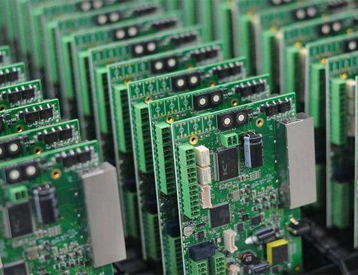
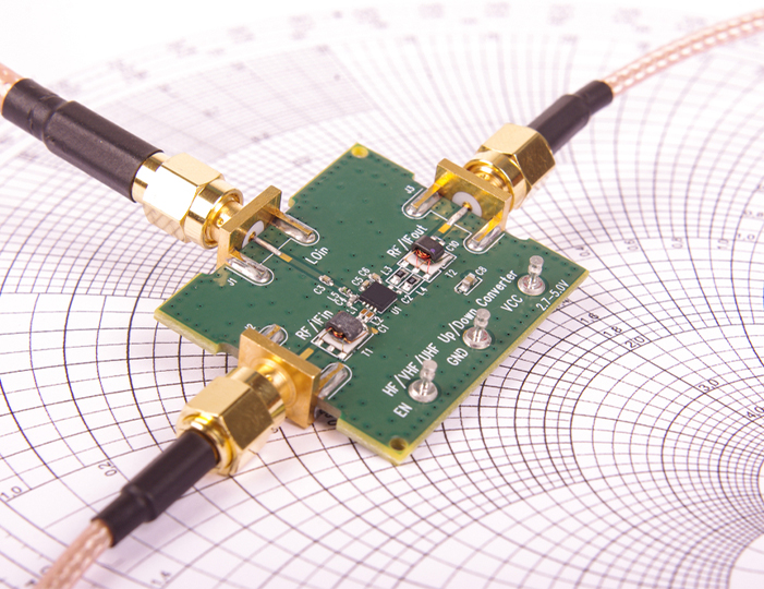
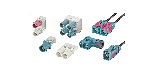
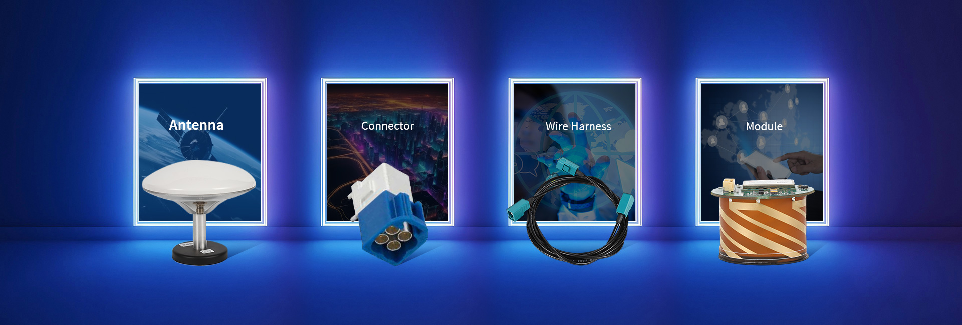
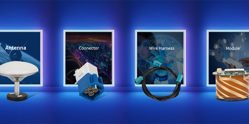
Products -PCBA Manufacturing RF Connectors RF Cable Assemblys Embedded Antennas External Antennas Positioning Chips and Modules
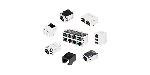
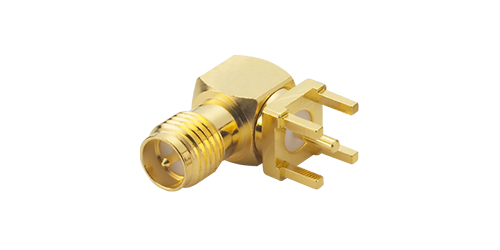
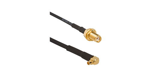
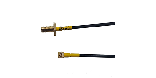
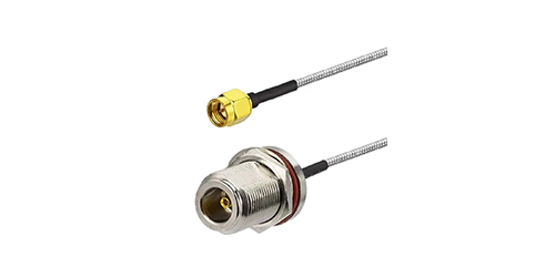
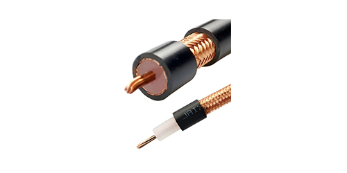
RF Connectors

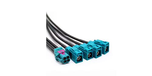
RF Cable Assemblys
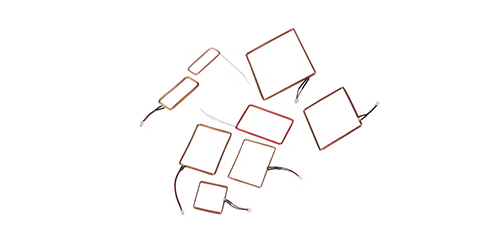
Embedded Antennas
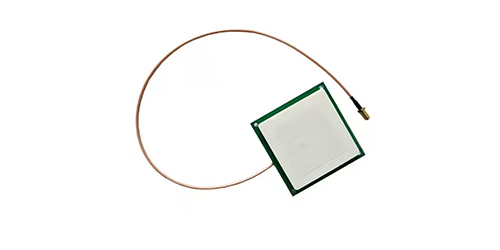
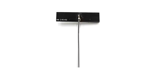
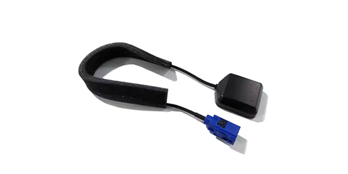
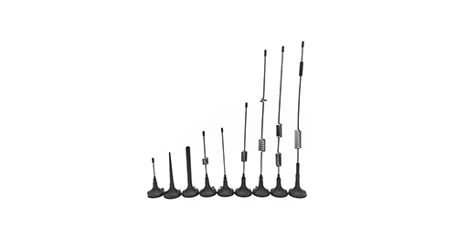
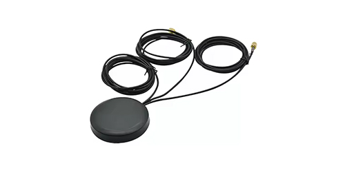
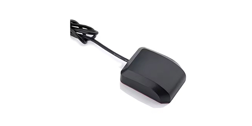
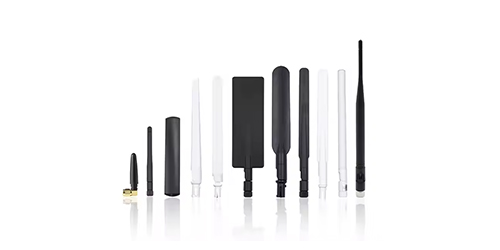
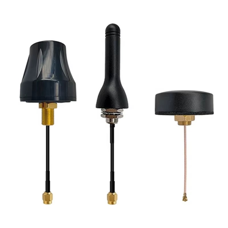
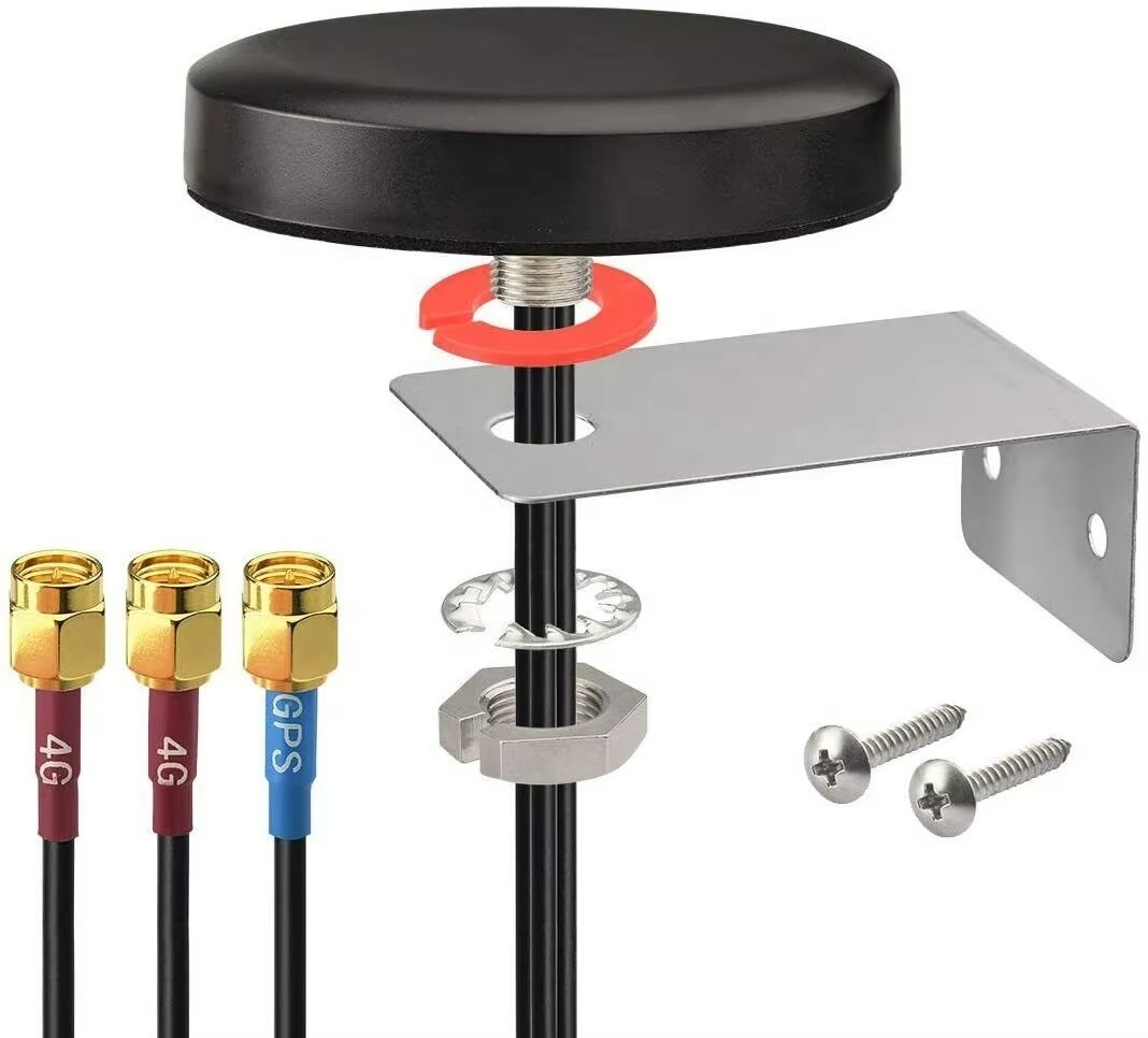
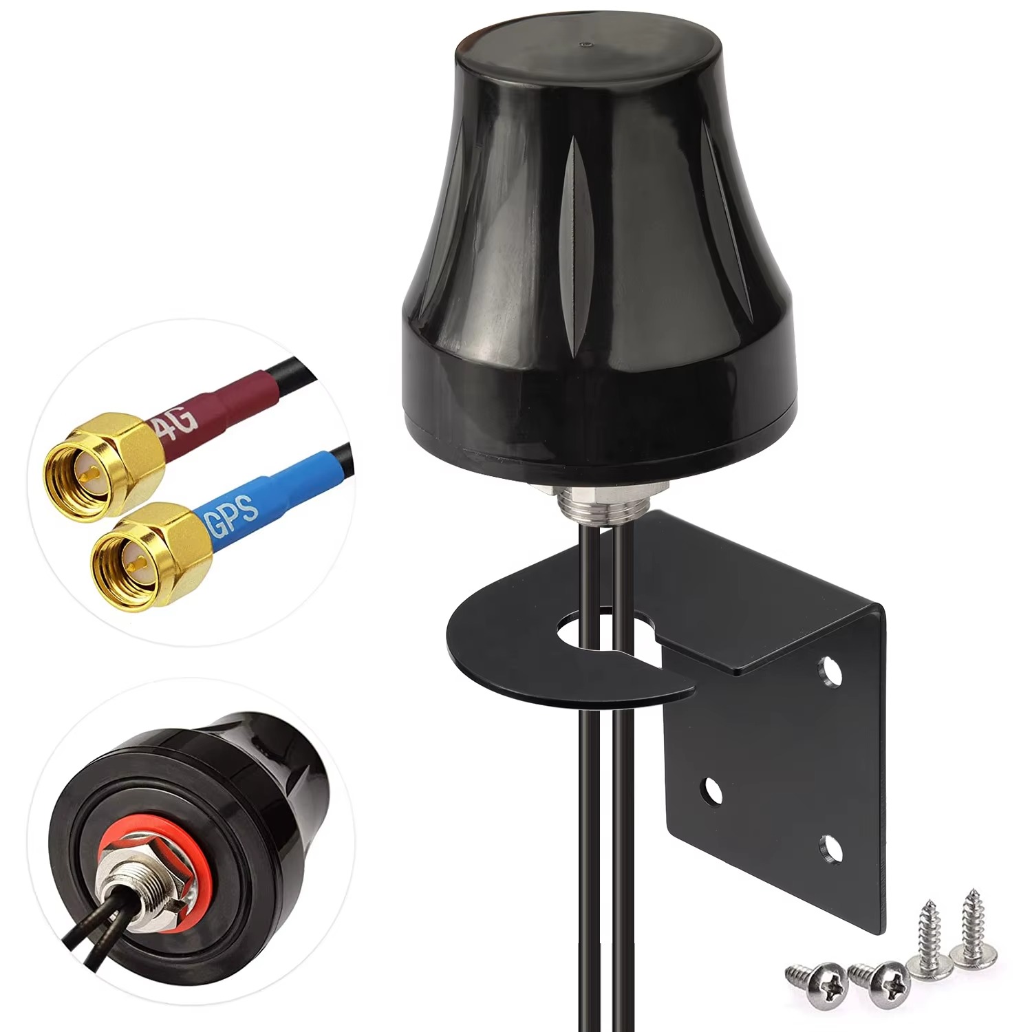
External Antennas
Positioning Chips and Modules
 Language


Language

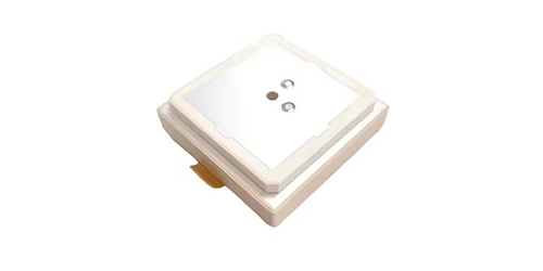
In the architecture of modern wireless devices, where every cubic millimeter is contested real estate, the antenna has undergone a radical transformation. The surface mount low-profile ceramic antenna represents the pinnacle of this evolution—a component that has been refined from a bulky, external accessory into a miniature, integrated, and automated-friendly module. This antenna is not merely an add-on; it is a fundamental building block of the Internet of Things (IoT), wearable technology, and ultra-slim consumer electronics, enabling wireless connectivity in forms previously deemed impossible.
A surface mount low-profile ceramic antenna is a type of patch antenna engineered for microwave frequencies—such as GNSS (L1, L5), Wi-Fi (2.4/5/6 GHz), Bluetooth, Zigbee, LTE, and 5G—that is manufactured as a standard Surface Mount Device (SMD). The "low-profile" designation typically refers to a height of less than 2mm, and often as slim as 0.6mm, allowing it to be mounted directly onto a printed circuit board (PCB) without contributing significantly to the device's z-height. The term "ceramic" denotes the use of a specialized high-dielectric-constant substrate, which is the key enabling technology that allows the antenna's physical dimensions to be a fraction of the wavelength it is designed to receive or transmit.
The primary role of this antenna is to act as the essential transducer between the guided electromagnetic waves traveling on the PCB's transmission lines and the free-space waves that carry data through the air. In a world demanding seamless connectivity, its function is to do this as unobtrusively as possible. It is the hidden conduit that allows a smartwatch to sync with a phone, a drone to receive GPS commands, an asset tracker to report its location via LTE-M, and a smartphone to connect to a Wi-Fi network, all without a visible antenna in sight.
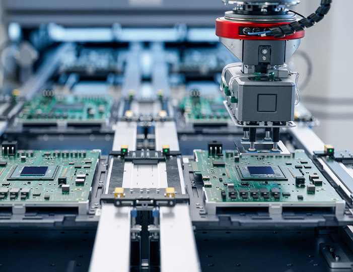
The driving force behind its development is the triple imperative of modern electronics: miniaturization, automated manufacturing, and cost-effectiveness. The surface-mount technology (SMT) format is non-negotiable for high-volume production; it allows pick-and-place machines to populate these antennas onto PCBs at incredible speeds alongside resistors, capacitors, and ICs, streamlining the assembly process and eliminating the need for manual soldering or connector attachment. This automation is crucial for producing millions of units consistently and reliably.
Furthermore, the proliferation of the IoT has created a market for billions of connected sensors and devices. These devices often have extreme space constraints and must be produced at the lowest possible cost. The ceramic SMD antenna meets this need perfectly, offering a blend of performance, size, and suitability for mass production that alternative solutions like etched PCB antennas or flexible printed circuit (FPC) antennas often cannot match in terms of consistency and integration ease.
However, this miniaturization and integration come with inherent engineering challenges. The laws of physics dictate that a smaller antenna has reduced bandwidth and lower efficiency compared to a larger one. The performance of these antennas is also highly sensitive to their immediate environment—the proximity of batteries, metal shields, and even the device's plastic housing can detune their resonant frequency. Therefore, successful implementation is not a simple component drop-in but requires careful RF co-design of the entire PCB and product enclosure.
In essence, the surface mount low-profile ceramic antenna is a masterpiece of compromise and precision engineering. It sacrifices some degree of raw performance for the supreme advantages of ultra-compact size, mechanical robustness, and seamless manufacturability. It is the unsung hero of the wireless revolution, a tiny ceramic tile that silently and reliably bridges the gap between the digital interior of our devices and the invisible networks that surround us, enabling the connected world we live in today.
The design and construction of a surface mount low-profile ceramic antenna is a meticulous process that blends advanced materials science with high-precision RF engineering. It is a multi-layered structure where every dimension, material property, and geometric feature is optimized to achieve target performance within a severely constrained physical volume, all while adhering to the rigors of automated assembly.
1. The Ceramic Substrate: The Foundation of Miniaturization
The core of the antenna is a monolithic block of engineered ceramic. This is not a generic material but a proprietary composite, often based on titanium ceramics or other complex oxides, sintered under high temperature and pressure to achieve specific electromagnetic properties:
High Dielectric Constant (εr): Values typically range from 10 to over 40. This is the key to miniaturization. A high εr reduces the wavelength within the material (λ_d = λ_0 / √εr), allowing the physical length of the radiating patch to be dramatically smaller for a given frequency. For example, an εr of 36 allows for a patch that is 6 times smaller than one in air.
Low Loss Tangent (tan δ): The material must have extremely low electromagnetic loss (tan δ < 0.002 is common). A high loss tangent would cause the antenna to dissipate transmitted power as heat within the ceramic itself, drastically reducing its radiation efficiency and effective range.
Temperature Stability: The dielectric constant must remain stable over the device's operating temperature range (e.g., -40°C to +85°C). Thermal drift would shift the antenna's resonant frequency, potentially moving it outside the desired communication band and causing link failure.
2. The Radiating Element: The Patch
A conductive radiating patch is fabricated on the top surface of the ceramic block. This is typically achieved through a thick-film printing process, where a silver- or copper-based conductive paste is screen-printed onto the raw ceramic substrate. The assembly is then fired in a kiln, fusing the metal to the ceramic to create a durable, low-resistance layer.
Patch Geometry: The patch is most commonly rectangular. Its length L is the primary determinant of the resonant frequency and is calculated to be slightly less than half the wavelength within the dielectric material (λ_d/2) at the target frequency.
Multi-Band Designs: To cover multiple bands (e.g., GPS L1 and L5, or Wi-Fi 2.4 and 5 GHz), more complex designs are employed:
Stacked Patches: A second, smaller parasitic patch on a separate ceramic layer is placed above the primary driven patch. The lower patch is tuned to the higher frequency, and the upper patch acts as a parasitic element for the lower frequency.
Slotted Patches: Inserting U-shaped or other slots of specific dimensions into the patch can perturb the surface current paths and create additional resonant modes, effectively enabling multi-band operation from a single feed point.
3. The Feed Mechanism: Connecting to the Board
The antenna must be connected to the RF transceiver on the host PCB. The two most common techniques are:
Probe Feed: A small pin (probe) is soldered to the patch and passes through a hole drilled in the ceramic to connect to a microstrip feedline on the host PCB. This is a robust and common method.
Aperture-Coupled Feed: A more advanced technique where the patch is on the top layer. Energy is coupled from a microstrip feedline on the host PCB through a slot etched in an intermediate ground plane. This offers better bandwidth and isolation between the feed network and the radiating element but is more complex.
4. The Ground Plane: A Critical External Dependency
Unlike some antennas, the ceramic patch antenna does not include its own ground plane. Instead, it is critically dependent on the ground plane of the host PCB. This copper pour on the PCB serves as the electrical counterpoise for the antenna. Its size, shape, and proximity are fundamental to the antenna's performance, directly influencing its bandwidth, efficiency, and radiation pattern. The antenna's datasheet will specify the minimum required ground plane dimensions for it to function as intended.
5. Final Packaging and SMT Termination
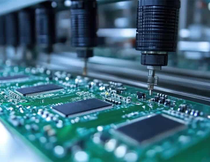
The final component is a single, monolithic ceramic block with metallization. The bottom side features solderable terminals (often using a Nickel barrier and a Gold flash over a Silver layer to ensure excellent solderability and prevent leaching). This SMT-compatible package allows it to be handled by standard pick-and-place machines. A solder paste stencil is used to apply paste to the PCB pads, the antenna is placed, and the entire board passes through a reflow oven, where the solder melts and forms a secure mechanical and electrical connection.
The entire construction process, from material formulation to final packaging, is geared towards creating a robust, consistent, and highly miniaturized component that can withstand the mechanical stresses of assembly and the environmental stresses of its operational life, all while delivering predictable RF performance.
The operation of a surface mount low-profile ceramic antenna is a practical application of resonant cavity theory, engineered into an ultra-compact form factor. Its working principle revolves around the efficient creation and radiation of a standing electromagnetic wave, a process that is fundamentally constrained by the antenna's miniature size and has profound implications for its performance and integration.
Fundamental Resonance in a Miniaturized Cavity
The antenna functions as a resonant cavity. The top metallized patch and the ground plane on the host PCB form the two conducting walls of this cavity. The space between them is filled with the high-dielectric ceramic substrate. When excited by an RF signal at its resonant frequency, electromagnetic fields oscillate within this cavity. The specific mode of operation is typically the TM₁₀ mode, where the electric field is oriented perpendicular to the patch and its magnitude varies sinusoidally across the patch's length. The "fringing fields" at the edges of the patch are responsible for coupling energy into free space, enabling radiation. The high dielectric constant of the ceramic effectively confines this resonance into a very small physical volume.
The Critical Role of the Host PCB's Ground Plane
The antenna's performance is not intrinsic; it is a collaborative effort with the host PCB. The PCB's ground plane is an active part of the antenna system. Its functions are:
Image Theory: The ground plane creates an electrical mirror image of the antenna below it. This effectively doubles the electrical height of the structure, which is crucial for achieving the desired radiation pattern and impedance.
Directionality: The ground plane shapes the radiation pattern, directing energy predominantly in the hemisphere above the board. This provides inherent rejection of signals arriving from below the horizon, which are often unwanted reflections (multipath).
Performance Determinant: The size of the ground plane directly controls the antenna's bandwidth. A larger ground plane generally supports a wider bandwidth. The antenna is designed with the assumption that this ground plane exists; without it, performance collapses.
The Inherent Trade-Off: Bandwidth vs. Size
The most significant operational characteristic of these antennas is their inherently narrow bandwidth. This is a direct consequence of the physics of miniaturization. The operational bandwidth of a resonant antenna is proportional to its electrical volume. By using a high-εr material to shrink this volume, the bandwidth is drastically reduced. Furthermore, a high Q-factor (Quality factor) associated with such a small resonant structure means it is tuned to a very specific frequency. For example, covering the entire 100 MHz required for the Wi-Fi 2.4 GHz band is a major design challenge. Techniques like slotting are used to create multiple resonances and broaden the effective bandwidth.
Environmental Sensitivity and the "Keep-Out" Zone
The antenna's performance is exquisitely sensitive to its immediate environment—a phenomenon known as detuning.
Proximity Effects: Any conductive or high-dielectric object near the antenna will alter its resonant frequency and impedance. This includes the device's battery, metal shields, displays, and even the user's hand. This can severely degrade performance, causing a mismatch that reduces radiated power and efficiency.
The Keep-Out Zone: To mitigate this, a strict keep-out area must be maintained around the antenna. This is a three-dimensional region on the PCB and within the device housing where no components, traces, or metal can be placed. Adherence to this guideline, specified by the antenna manufacturer, is absolutely critical for achieving the desired performance.
The Complete Signal Path
The device's RF transceiver generates a signal, which travels via a controlled-impedance microstrip trace on the PCB to the antenna's feed point.
This signal excites the ceramic patch, setting up a standing wave within the dielectric cavity.
The fringing fields at the edges of the patch couple energy into free space, radiating an electromagnetic wave.
For reception, the process is reversed: an incoming wave induces currents on the patch, which are transferred through the feed point to the transceiver's low-noise amplifier.
In summary, the surface mount ceramic antenna works by concentrating a resonant electromagnetic mode into a tiny volume. Its principle of operation is a constant balance act, trading bandwidth for size and requiring a symbiotic relationship with its host PCB and a carefully controlled environment to function as intended.
The surface mount low-profile ceramic antenna offers a compelling set of advantages that have cemented its role in modern electronics manufacturing. However, reaping these benefits requires a clear understanding of and careful management of its inherent limitations and integration challenges.
Advantages
Ultra-Low Profile and Miniaturization: This is the defining advantage. With heights often below 1.5mm, these antennas enable the design of incredibly thin devices like smartphones, wearables, and IoT sensors where z-height is a primary constraint. They are a key enabler of the sleek, minimalist industrial designs that dominate the market.
Surface-Mount Technology (SMT) Compatibility: This is a massive advantage for manufacturing. As standard SMD components, they are perfectly suited for fully automated, high-volume PCB assembly. They can be picked, placed, and reflow-soldered by machines at high speed alongside resistors and capacitors, drastically reducing assembly time, cost, and potential for human error compared to installing a separate antenna with a connector.
Mechanical Robustness and Reliability: The monolithic ceramic structure is extremely rigid, resistant to mechanical shock, vibration, and deformation. Once soldered to a PCB, they form a very durable connection that is far more robust than a flexible printed circuit (FPC) antenna attached with adhesive, which can peel or be damaged. They can withstand the high temperatures of the reflow soldering process without damage.
Performance Consistency and Repeatability: Being a pre-fabricated, characterized component, their performance is highly consistent from one unit to the next. This eliminates the variability that can be introduced by the etching process for PCB trace antennas or the placement accuracy of FPC antennas. This leads to higher manufacturing yield and more predictable RF performance in the final product.
Good Performance for Size: Within their class, they offer excellent performance for a given volume. Their radiation efficiency, while lower than a large external antenna, is often superior to other integrated antenna solutions (like etched PCB antennas) in the same footprint due to the stable properties of the ceramic material and its isolation from board-level noise.
Design Flexibility: They are available in a vast array of standardized sizes and frequency bands from multiple manufacturers. This allows designers to select an off-the-shelf component that meets their needs without undertaking a custom antenna design project.
Challenges and Limitations
Inherently Narrow Bandwidth: This is the most significant technical drawback. The high dielectric constant needed for miniaturization inherently reduces bandwidth. Covering wide modern bands (e.g., the 600 MHz required for Wi-Fi 6E) is extremely challenging and often requires multiple antennas or complex, costly multi-resonant designs.
High Sensitivity to Integration Environment (Detuning): The antenna's performance is not guaranteed by the component itself. It is critically dependent on the host PCB's ground plane and the surrounding components. The proximity of batteries, displays, metal shields, and even the plastic housing can capacitively load the antenna, shifting its resonant frequency and degrading its performance. This makes the design process iterative and complex.
Dependence on Host PCB Design: The antenna requires a specific ground plane on the host PCB to function correctly. The product's PCB layout must be carefully designed to provide this ground plane exactly as specified by the antenna manufacturer. Any deviation will severely impact performance. This couples the RF design tightly to the board layout.
Lower Efficiency Compared to Larger Antennas: Due to their small size and dielectric losses, their radiation efficiency is inherently lower than that of a larger external antenna. This translates to reduced range and weaker signal strength for both transmission and reception. A device may require more transmit power to achieve the same range, negatively impacting battery life.
Cost: High-quality ceramic materials with precise dielectric properties are more expensive than standard PCB laminates like FR4. The manufacturing process for the antenna itself is also more complex than printing a trace on a PCB. Therefore, a ceramic antenna component has a higher unit cost than an integrated printed antenna.
Complex Design-In Process: Successfully integrating a ceramic antenna is not a simple component drop-in. It requires expert RF design knowledge, careful PCB layout (including the critical keep-out area), and extensive testing in the final product enclosure with all components installed. This often necessitates multiple design iterations and prototyping cycles, adding time and non-recurring engineering (NRE) cost to the product development process.
In conclusion, the advantages of the surface mount ceramic antenna are overwhelmingly centered on enabling miniaturization and automated manufacturing. The challenges are primarily performance-related and demand careful engineering management. The decision to use one is a strategic trade-off, choosing the benefits of a standardized, robust, and tiny component over the raw performance of a larger solution and accepting the integration complexity that comes with it. For the vast majority of high-volume consumer and IoT devices, this is a trade-off well worth making.
The surface mount low-profile ceramic antenna is a foundational technology that enables wireless connectivity across a breathtakingly diverse range of modern electronic devices. Its unique combination of miniaturization, performance, and manufacturability has made it the default choice for applications where space is at a premium and production volume is high. As technology evolves, its applications continue to expand, and the antenna itself is undergoing significant innovation to meet future demands.
Applications
Smartphones, Tablets, and Laptops: This is the highest-volume application. A single modern smartphone contains multiple ceramic antennas for different services: primary and diversity cellular antennas for 4G/5G, Wi-Fi/Bluetooth, GPS/GNSS, and sometimes NFC. Their low profile is essential for the all-screen, bezel-less designs that dominate the market. They are often placed in the narrow bezels or within the device's mid-frame.
Wearable Technology: Smartwatches, fitness trackers, and wireless earbuds have perhaps the most severe space constraints. A ceramic antenna is often the only viable solution for integrating Bluetooth, Wi-Fi, or GPS connectivity into these tiny form factors without adding noticeable thickness or compromising water resistance.
Internet of Things (IoT) Modules and Sensors: The IoT revolution is fueled by these antennas. They are used on compact IoT modules for protocols like:
Cellular IoT: LTE-Cat M1 (CAT-M), NB-IoT.
LPWAN: LoRaWAN, Sigfox.
Short-Range: Wi-Fi, Bluetooth Low Energy (BLE), Zigbee.
This enables wireless functionality in devices like asset trackers, smart meters, environmental sensors, agricultural monitors, and industrial safety equipment.
Consumer Electronics: A wide array of products rely on them, including:
TVs and Set-Top Boxes: For Wi-Fi and Bluetooth connectivity.
Smart Home Devices: Voice assistants (e.g., Amazon Echo, Google Nest), smart thermostats, and security cameras.
Gaming: VR/AR headsets and game controllers.
Digital Cameras: For Wi-Fi photo transfer.
Automotive Electronics: Modern vehicles are rolling networks. Ceramic antennas are used in telematics control units (TCUs), tire pressure monitoring systems (TPMS), keyless entry fobs, and infotainment systems for GPS and cellular connectivity. Their robustness is key to surviving the automotive environment.
Medical Devices: Portable medical devices and patient monitors use them for wireless data transfer. Wearable health monitors (e.g., ECG patches, continuous glucose monitors) leverage their small size for patient comfort and discretion.
Future Trends
Multi-Band and Wideband Designs for 5G and Wi-Fi 6/7: The demand for higher data rates is pushing antennas to cover wider bands. Future ceramic antennas will use more advanced techniques:
Advanced Stacking: Multi-layer ceramics with more complex stacked patches to cover multiple wide bands (e.g., all of 5G FR1 n77/n78/n79 bands).
Meta-Materials: Incorporating electromagnetic band-gap (EBG) structures or other meta-material concepts to effectively create a "larger" antenna electrically, thereby increasing bandwidth without increasing physical size.
Antenna-in-Package (AiP) and System-in-Package (SiP): This is a major paradigm shift. The ceramic antenna will be co-packaged with the RF transceiver chip, filters, and other components into a single, pre-tested module. This simplifies design for the end customer, reduces the overall footprint, minimizes parasitic effects from interconnects, and improves overall system performance. This is already happening for mmWave 5G antennas.
Integrated Passive Devices (IPDs): Antenna manufacturers will move beyond single components to offer entire "antenna solutions" on a single ceramic substrate, integrating matching networks, filters, and baluns alongside the radiating element. This further reduces the component count and board space required.
Tuning and Adaptive Impedance Matching: To combat detuning from environmental effects (e.g., a user's hand), future antennas will incorporate active tuning elements. Using tunable capacitors (varactors) or switchable matching networks, the antenna's impedance can be dynamically adjusted in real-time to maintain an optimal match, maximizing efficiency and data throughput.
Material Science Innovations: Research into new ceramic and composite materials continues. Goals include developing dielectrics with an even higher εr for further miniaturization, a more stable temperature coefficient, and a better balance between high εr and low loss tangent to improve efficiency.
Co-Design with AI and Machine Learning: The use of AI in electromagnetic simulation software will accelerate the antenna design process. Machine learning algorithms can rapidly iterate through thousands of potential geometric configurations to automatically optimize for specific goals like bandwidth, efficiency, or size, dramatically reducing design time and pushing the performance boundaries of these tiny components.
The surface mount low-profile ceramic antenna is a dynamically evolving technology. Its future is one of greater integration, intelligence, and performance, ensuring it remains the cornerstone of wireless connectivity for the next generation of ever-smaller, smarter, and more connected devices.
Conclusion
The surface mount low-profile ceramic antenna stands as a testament to the triumph of integration and miniaturization in electronic design. It is far more than a simple component; it is a critical enabler that has allowed form factor to become a primary driver of innovation in consumer electronics and the Internet of Things. By solving the once-intractable problem of where to put the antenna, it has empowered designers to create the sleek, seamless, and wireless devices that define our modern experience.
Its design and construction represent a masterful application of materials science. The strategic use of high-dielectric-constant ceramics is the fundamental breakthrough, allowing engineers to effectively "bend" the rules of antenna physics to fit a resonant structure into a space previously considered unusable for RF purposes. This core innovation is complemented by manufacturing processes that ensure robustness, consistency, and compatibility with the high-speed automated assembly lines that produce our gadgets.
The analysis of its advantages and limitations reveals its true character: it is the optimal solution for a world prioritizes size and manufacturability. Its unparalleled suitability for SMT assembly and its mechanical durability are overwhelming advantages for mass production. The challenges it presents—primarily limited bandwidth and environmental sensitivity—are not shortcomings but rather the well-defined parameters of its operation. They are the known constraints that skilled RF engineers must design around, a trade-off that is overwhelmingly justified by the aesthetic and functional benefits of ultra-compact design.
The antenna's working principle, a marvel of miniaturized resonance, highlights the sophisticated trade-offs at play. It acknowledges that maximum efficiency and bandwidth must be relinquished to achieve minimal volume, but it does so in the most optimized way possible, extracting the highest possible performance from every cubic millimeter of ceramic.
Looking forward, the trajectory of this technology is not towards obsolescence but towards greater intelligence and integration. Trends like Antenna-in-Package (AiP) and adaptive tuning are not threats but natural evolutionary steps that will further blur the line between the antenna and the rest of the RF front-end, simplifying design and enhancing performance. It will continue to be the hidden workhorse, embedded within the devices of the future, silently providing the essential link to the wireless world.
In conclusion, the surface mount low-profile ceramic antenna is a cornerstone of modern electronics. It is a powerful example of how a focused solution to a specific engineering challenge—the need for invisible, reliable wireless connectivity—can have an outsized impact on entire industries. By conquering the problem of space, it has ensured that the devices of the future can be both beautiful and connected, without compromise. It is a small component that has made, and continues to make, a very large possible.

 86 0755 2819 9597
Lucy Yang | lucy.y@toxutech.com
Nicole Li | nicole@toxutech.com
Dotty Zhao | sales04@toxutech.com
Global Business Director / Sales Team / Global Operations


 En
En Cn
Cn Korean
 Home >


