

-
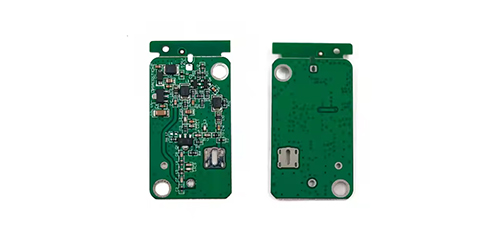
Products -PCBA Manufacturing RF Connectors RF Cable Assemblys Embedded Antennas External Antennas Positioning Chips and Modules
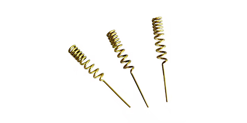
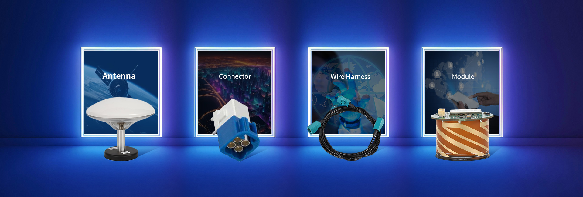
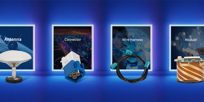
RF Connectors

RF Cable Assemblys
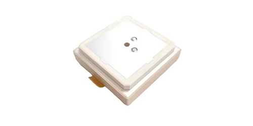
Embedded Antennas
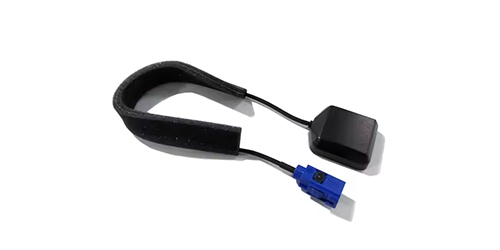
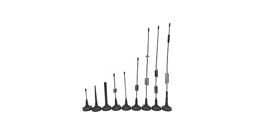
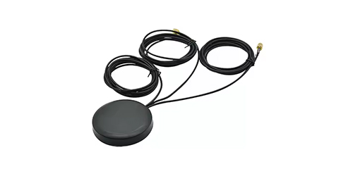
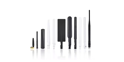
External Antennas
Positioning Chips and Modules

 Language


Language

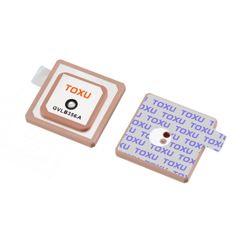
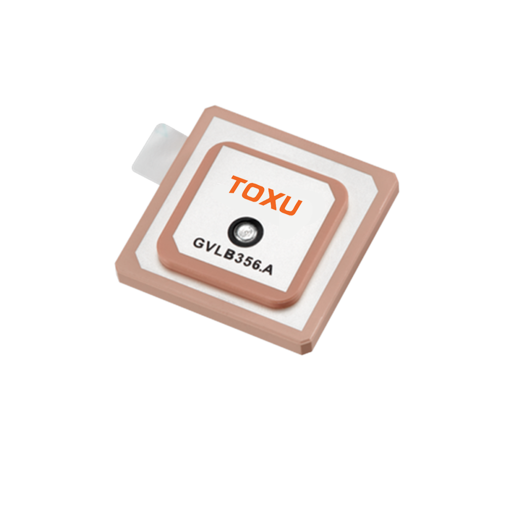
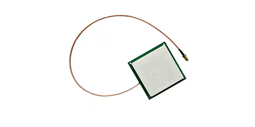
In the vast and invisible landscape of radio frequency (RF) signals, the antenna serves as the critical gateway, the transducer that converts electromagnetic waves propagating through space into electrical currents that can be processed by a circuit. Within the realm of Global Navigation Satellite Systems (GNSS), which includes GPS, GLONASS, Galileo, and BeiDou, antennas are the first and most vital link in the chain of determining a position. Among the diverse types of GNSS antennas, the Surface-Mount Device (SMD) passive GPS ceramic antenna has emerged as the ubiquitous, miniature workhorse, enabling location capabilities in an astounding array of consumer and industrial products.
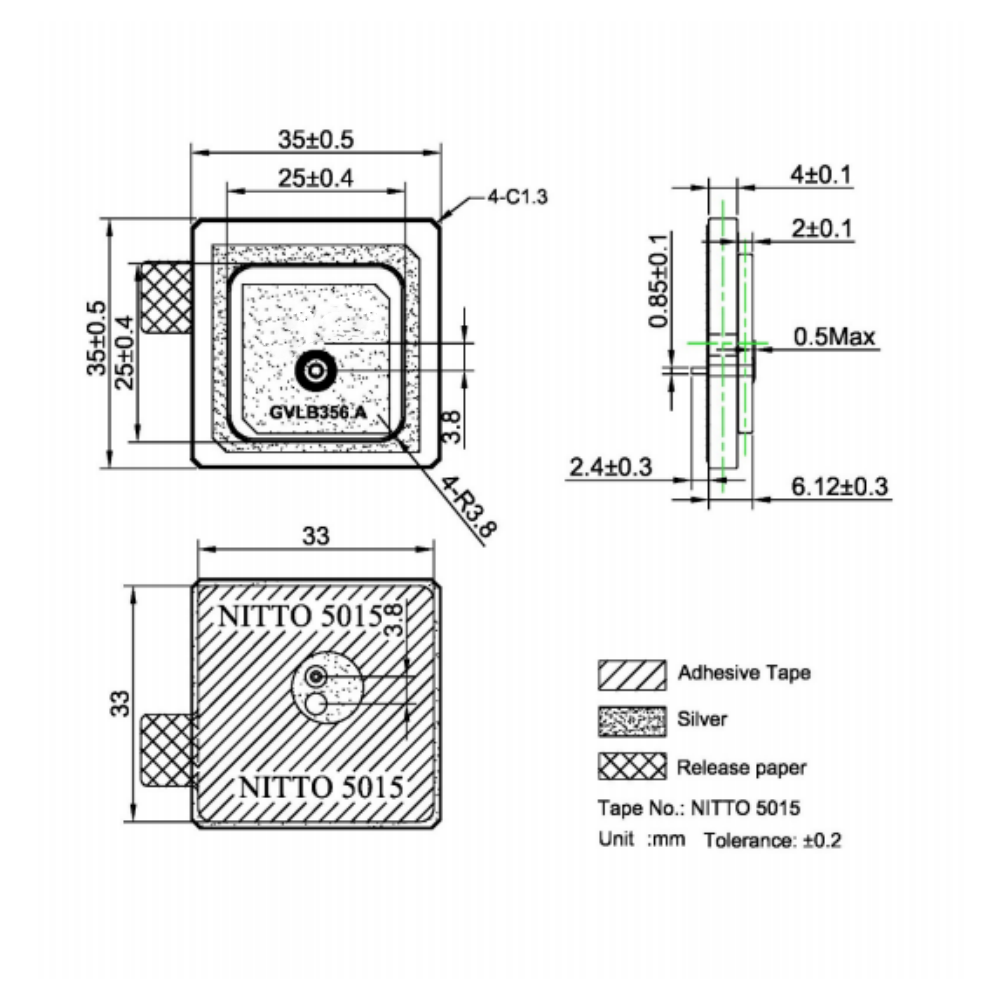
An SMD passive GPS ceramic antenna is a type of antenna specifically designed for receiving GNSS signals, characterized by three key attributes:
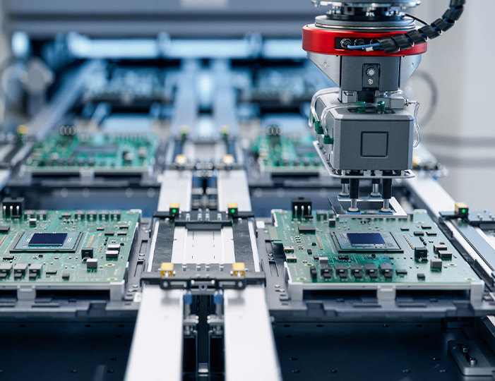
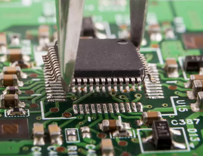
Surface-Mount Device (SMD): It is built to be mounted directly onto the surface of a printed circuit board (PCB) using reflow soldering techniques. This allows for high-volume, automated assembly, making it ideal for mass-produced electronics. It eliminates the need for connectors, cables, and manual labor, significantly reducing the size, cost, and complexity of integration.
Passive: It contains no active electronic components, such as a Low-Noise Amplifier (LNA). It is a purely passive radiating element. This means it does not require a power source. While this simplifies design and reduces cost, it also means the signal it delivers to the receiver is very weak and susceptible to degradation from transmission losses in the circuit board traces and connectors.
Ceramic: The core radiating element is crafted from a specialized ceramic material with a high dielectric constant (εr). This high permittivity allows the electromagnetic waves to wavelength within the ceramic, enabling the creation of a physically small antenna that is electrically resonant at the target GNSS frequencies (e.g., 1575.42 MHz for GPS L1).
The proliferation of these antennas is a direct consequence of the miniaturization and cost-reduction pressures in the electronics industry. As GPS evolved from a specialized military and surveying tool into a standard feature in smartphones, wearables, drones, asset trackers, and Internet of Things (IoT) devices, the antenna had to shrink from a large, external component with a connector into a tiny, cheap, and reliable chip that could be soldered inside a device's often crowded enclosure.
The primary advantage of the SMD ceramic antenna is its incredibly small form factor and low cost. It can be integrated seamlessly into a product's PCB layout, hidden from the user, and requires no external assembly. This makes it the default choice for space-constrained and cost-sensitive applications where ultimate performance is secondary to size, price, and ease of manufacturing.
However, this convenience comes with significant engineering challenges. Unlike an active external antenna with a dedicated, controlled environment, a passive SMD antenna's performance is deeply intertwined with the PCB it is mounted on. The PCB itself becomes part of the antenna system. The size and shape of the board, the placement of the antenna on it, the proximity of other components (especially noise-emitting processors and radios), and the composition of the device's plastic casing all have a profound impact on its efficiency, bandwidth, and radiation pattern. A poor implementation can render a well-designed antenna nearly useless, leading to weak signal reception, long time-to-first-fix (TTFF), and unreliable positioning.
Therefore, the SMD passive ceramic antenna is not merely a component one simply solders onto a board; it is a system whose performance is dictated by the entire design of the host product. It represents a triumph of miniaturization and manufacturing efficiency, but it also demands careful RF design discipline to unlock its potential. It is the silent enabler of location awareness in the modern world, a tiny ceramic speck that listens to the heavens from the palm of your hand.
The operation of an SMD passive GPS ceramic antenna is governed by the fundamental principles of antenna theory, miniaturized and adapted for integration onto a circuit board. Its primary job is to efficiently resonate at the GNSS L1 frequency, capture the incoming electromagnetic energy, and transfer it as an electrical current to the receiver with minimal loss.
1. Resonance: The Key to Reception
An antenna is essentially a resonant structure, like a tuning fork for radio waves. It is designed to be electrically resonant at a specific frequency—in this case, 1575.42 MHz. At resonance, the antenna's impedance is purely resistive (ideally 50 ohms) and its reactance (the imaginary part of impedance) is zero. This is the condition for maximum power transfer from free space into the antenna's terminals. The high-dielectric ceramic material enables this resonance to occur in a physically small structure by effectively "slowing down" the electromagnetic waves, allowing a shorter path length to achieve the required electrical length for resonance.
2. The Role of the Ground Plane
As established, the antenna cannot work alone. The RF currents flowing on the ceramic radiating element induce corresponding "image currents" on the PCB's ground plane. These currents cause the ground plane to radiate as well. The combination of the ceramic element and the ground plane together forms the complete radiating structure. The radiation pattern is not a perfect sphere but is typically directed away from the ground plane. This is actually beneficial in most devices, as the ground plane and other components are often on one side, so the antenna radiates best out the "open" side of the device (e.g., the top of a smartphone or the sky-facing side of a drone).
3. Impedance Matching: The Handshake
For maximum power transfer, the impedance of the antenna must match the impedance of the transmission line (the PCB trace) and the input impedance of the GNSS receiver chip, which is almost universally 50 ohms. The PIFA design, with its integrated shorting pin, is inherently easier to match to 50 ohms than a simple patch. However, perfect matching is rarely achieved directly at the antenna's feed point. Therefore, a matching network is almost always required.
This matching network is a small circuit, typically consisting of inductors and capacitors (L-C network), placed on the PCB between the antenna feed pad and the receiver. This network transforms the antenna's complex impedance (which may be, for instance, 15 + j25 ohms) to as close to 50 + j0 ohms as possible. The design of this network is critical and must be finalized after the antenna's placement on the final PCB layout has been tested, as the surrounding environment affects the impedance.
4. The Challenge of Bandwidth
GNSS signals themselves have a narrow bandwidth, but a modern receiver may want to receive signals from multiple constellations (GPS, Galileo, etc.) that are slightly offset in frequency. Furthermore, the antenna's resonant frequency can shift due to manufacturing tolerances, temperature changes, and proximity to other materials (like a plastic case). Therefore, the antenna must have adequate bandwidth—typically at least 10-20 MHz—to cover these frequencies and accommodate potential shifts. The bandwidth of a small antenna is inherently narrow due to its high Q factor. Designers work to widen the bandwidth through techniques like multi-layer electrode design or carefully controlled losses in the ceramic material.
5. Radiation Pattern and Efficiency
The radiation pattern of a PCB-mounted ceramic antenna is often irregular and hemisphere-like. It is not a primary concern for most consumer devices, as they are used in random orientations. The key metric is radiation efficiency—the ratio of power radiated by the antenna to the power accepted at its terminals. This efficiency is always less than 100% due to losses:
Dielectric Loss: Energy lost as heat within the ceramic material.
Conductor Loss: Resistance in the silver electrodes.
Ground Plane Loss: Inefficiencies in the PCB's copper.
Impedance Mismatch Loss: Power reflected back to the source due to poor matching.
A well-designed implementation might achieve 50-70% efficiency (-3 to -1.5 dB), while a poor one can be below 25% (-6 dB), meaning over 75% of the precious signal power is lost before it even reaches the receiver.
In essence, the antenna works by resonating in sympathy with the incoming satellite signals, capturing their energy, and, with the crucial help of its ground plane, delivering that energy through a carefully matched pathway to the receiver's highly sensitive input stage.
The decision to use an SMD passive ceramic antenna is a calculated engineering trade-off, offering compelling advantages for mass production while introducing significant design challenges that must be meticulously managed.
Advantages:
Extreme Miniaturization: This is the foremost advantage. Their tiny size (e.g., 10x10x3 mm) allows them to be integrated into increasingly compact devices like wearables, trackers, and miniature modules where any external antenna is impossible.
Low Cost: Mass-produced using standard ceramic and electrode printing processes, these antennas are extremely inexpensive, often costing just a few cents to a dollar per unit in volume. This is critical for consumer goods where every component cost is scrutinized.
Ruggedness and Reliability: Being a solid block of ceramic soldered directly to the PCB, they are highly resistant to vibration, shock, and physical wear and tear. There are no cables to break or connectors to become loose or corroded.
Ease of Assembly: As surface-mount components, they are perfectly suited for fully automated PCB assembly using pick-and-place machines and reflow ovens. This eliminates manual soldering or assembly steps, reducing manufacturing time and cost and improving consistency.
Aesthetics and Design Freedom: They are hidden inside the device's enclosure, allowing industrial designers to create sleek, unbroken product forms without external protrusions or specific "antenna lines."
Passive Operation: They require no power supply or bias tee circuitry, simplifying the overall system design and consuming zero power.
Challenges:
Performance Dependency on Host PCB: This is the single greatest challenge. The antenna's performance is wholly dependent on the PCB design. The size, shape, and layout of the ground plane are the most critical factors. A poor ground plane design is the most common cause of failure.
Sensitivity to the Local Environment: The antenna's performance can be severely degraded by nearby objects. This includes:
Components: Batteries, LCD screens, cameras, and metal shields can detune the antenna if placed too close.
Human Body (Hand Effect): The human body is mostly water, which absorbs RF energy. When a hand grips a device, it can block the antenna's radiation pattern and load it, shifting its resonance and killing performance. This is a major challenge for smartphones and wearables.
Device Casing: The plastic enclosure around the antenna has a dielectric constant that will affect performance. The antenna must be designed and tuned with the specific casing material and distance in mind.
Lower Efficiency and Gain: Compared to an active external antenna with a clear view of the sky, a passive internal antenna inherently has lower efficiency due to its small size and losses in the surrounding environment. This results in a lower Gain-to-Noise-Temperature (G/T) ratio, which can impact performance in weak signal conditions (e.g., indoors or in urban canyons).
Complex Design and Tuning Process: Integrating one of these antennas is not a simple "drop-in" task. It requires:
Careful PCB Stack-up Design: Ensuring continuous ground planes on adjacent layers.
Strategic Placement: Locating the antenna in a corner or at the edge of the board, away from noise sources and large obstructive components.
Post-Layout Tuning: The matching network (L-C values) must be optimized on the final physical board with its enclosure. This requires an RF testing setup (vector network analyzer) and expertise.
Susceptibility to Noise: The antenna's location on the main PCB puts it in close proximity to digital noise sources like processors, memory, and other radios (cellular, WiFi, Bluetooth). This noise can easily couple into the antenna and drown out the extremely weak GNSS signals, which are billions of times weaker. Careful filtering and shielding are mandatory.
Narrow Bandwidth: Their small size makes it challenging to design them for wide bandwidth, which is increasingly important for receiving multiple GNSS bands (L1, L2, L5) for high-precision applications.
In conclusion, the advantages of cost, size, and manufacturability make SMD ceramic antennas the only choice for countless applications. However, these benefits are unlocked only by accepting the challenge of a complex, system-level RF design process that treats the entire PCB as part of the antenna.
The SMD passive ceramic antenna has become the cornerstone of ubiquitous, low-cost positioning, finding its way into a staggering variety of applications. Its future evolution is driven by the demands of these applications and the relentless march of technology.
Applications:
Smartphones and Tablets: The primary driver of volume. Every smartphone contains at least one of these antennas for GNSS, often housed in the top or bottom bezel of the device. Designers face a constant battle to maintain performance despite metal frames, large screens, and the presence of the user's hand.
Wearable Devices: Fitness trackers, smartwatches, and personal locator beacons rely on these tiny antennas to provide location data. The extreme size constraints and the severe impact of the human body make this the most challenging application.
Asset Tracking and IoT: This is a massive growth area. Small, low-power trackers for logistics, supply chain management, and theft prevention use these antennas to report their position over cellular (LTE-M/NB-IoT) or satellite (Iridium, Globalstar) networks.
Drones and Robotics: Small consumer and professional drones use SMD antennas for their flight controllers and, in some cases, for the GNSS receiver. Their small size and weight are critical here.
In-Vehicle Telematics and Usage-Based Insurance (UBI): Small dongles or embedded modules that plug into a car's OBD-II port use these antennas to track vehicle location and driving behavior.
Consumer Electronics: Digital cameras (for geotagging), portable gaming devices, and personal navigation devices have historically used them.
General Purpose GNSS Modules: Many "plug-and-play" GNSS receiver modules aimed at designers and hobbyists come with a pre-integrated and pre-tuned ceramic antenna, simplifying the design process for end products.
Future Trends:
Multi-Band Support: The future of high-accuracy GNSS lies in using multiple frequency bands (L1 + L5) to correct for ionospheric delay. The major challenge is designing a tiny, passive antenna that can operate efficiently across two very separate frequency bands (1575 MHz and 1176 MHz). This involves innovative designs like coupled resonators and more complex multi-layer structures.
Enhanced Resilience to Detuning: Research is focused on designs that are less sensitive to the effects of the human body and nearby materials. Techniques include using balanced (differential) feed designs or incorporating passive parasitic elements that help stabilize the antenna's performance parameters.
Integration with Other Technologies:
AiP (Antenna-in-Package): The next step in miniaturization is to move the antenna from the main PCB directly into the same IC package as the GNSS receiver chip itself. This would save even more space and simplify design but presents immense challenges in isolating the antenna from the noise of the silicon die.
Hybrid Antennas: Combining a ceramic antenna structure with other materials or using the device's metal frame as part of the radiating element to improve efficiency and bandwidth.
Improved Simulation and Design Tools: As EM simulation software becomes more powerful and accessible, it will allow designers to more accurately model the entire system—antenna, PCB, enclosure, and human body—before building physical prototypes, reducing design cycles and improving first-pass success.
Materials Development: The search for ceramic materials with even higher dielectric constants and lower loss tangents continues, promising further miniaturization or efficiency improvements for a given size.
The SMD passive ceramic antenna will remain the dominant solution for mass-market GNSS for the foreseeable future. Its evolution will be characterized not by displacement by a new technology, but by its continued adaptation to become more robust, more broadband, and even more deeply integrated into the electronic systems it enables.
Conclusion
The SMD passive GPS ceramic antenna is a paradigm of modern electronics: a component whose profound impact is inversely proportional to its physical size. It is a masterpiece of engineering trade-offs, sacrificing the raw performance of a large, external antenna for the unparalleled benefits of miniaturization, cost-effectiveness, and seamless integrability. This trade-off has been the fundamental enabler of the location-aware revolution, transforming GNSS from a specialized tool into a ubiquitous utility embedded in billions of devices.
Its success, however, is not inherent to the component itself but to the system it commands. The central lesson of this antenna is that it is not a standalone part but the nucleus of a larger radiating structure whose performance is dictated by the entire printed circuit board and the device that houses it. It demands respect and expertise from the design engineer. It punishes casual implementation with failed projects and poor performance, but it rewards careful, disciplined RF design with reliable, cost-effective functionality.
The challenges it presents—sensitivity to environment, body detuning, low efficiency, and noise susceptibility—are not flaws but rather defining characteristics of its ultra-compact form factor. They are the price paid for the convenience of having a powerful navigational receiver inside a smartwatch or a phone. These challenges continue to drive innovation in materials science, electromagnetic design, and simulation methodologies.
Looking ahead, the role of the SMD ceramic antenna is secure. As the Internet of Things expands and location context becomes ever more critical to autonomous systems and personal electronics, the demand for small, cheap, and reliable antennas will only grow. The future will see them evolve to become more resilient, more versatile across multiple GNSS frequencies, and more deeply integrated into the silicon of the chips they serve. They are the unseen, unheralded gateways that connect our miniature electronic worlds to the constellation of satellites soaring overhead, silently and ceaselessly telling us where we are.

 86 0755 2819 9597
Lucy Yang | lucy.y@toxutech.com
Nicole Li | nicole@toxutech.com
Dotty Zhao | sales04@toxutech.com
Global Business Director / Sales Team / Global Operations


 En
En Cn
Cn Korean
 Home >


