

-
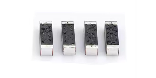
Products -PCBA Manufacturing RF Connectors RF Cable Assemblys Embedded Antennas External Antennas Positioning Chips and Modules
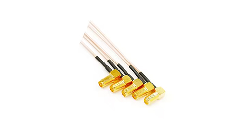
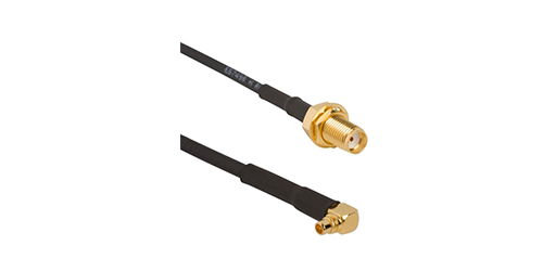
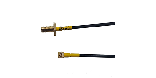
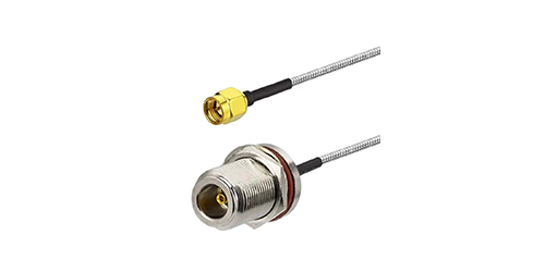
RF Connectors

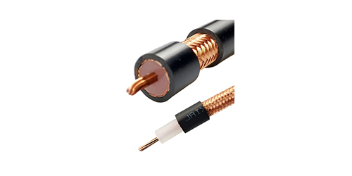
RF Cable Assemblys
Embedded Antennas
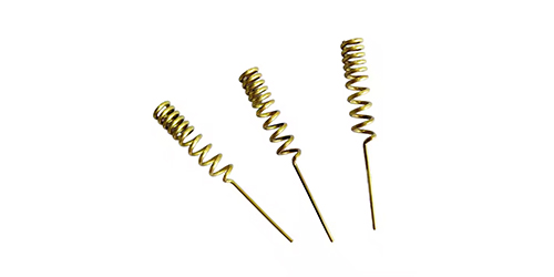
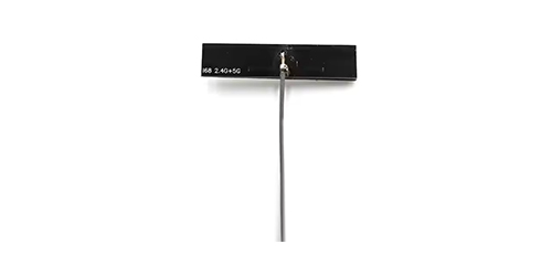
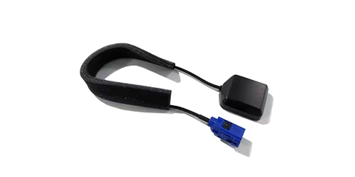
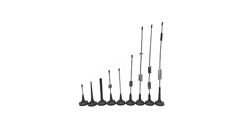
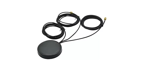
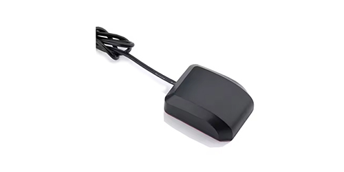
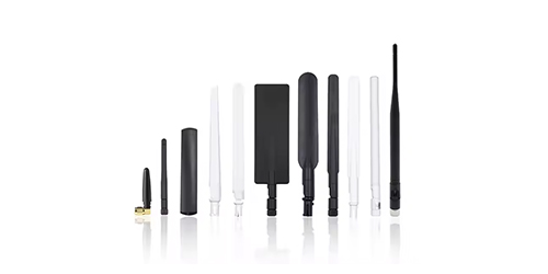
External Antennas
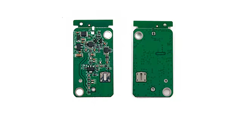
Positioning Chips and Modules


 Language


Language


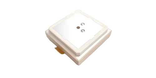
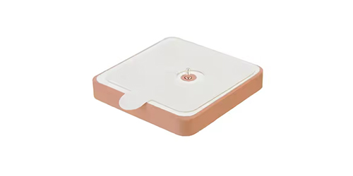
Surface-Mount Device (SMD) GPS antennas represent a critical innovation in the field of satellite positioning technology, specifically tailored to meet the demands of modern compact electronic devices. As the global market for portable gadgets—such as smartphones, wearables, IoT sensors, and miniaturized industrial trackers—continues to expand, the need for small, lightweight, and high-performance positioning components has become increasingly urgent. Traditional GPS antennas, often bulky and requiring external mounting, struggle to fit within the sleek, space-constrained designs of today’s electronics. SMD GPS antennas address this gap by leveraging surface-mount technology, which allows them to be directly soldered onto printed circuit boards (PCBs), eliminating the need for extra mounting hardware and significantly reducing their footprint.
At their core, SMD GPS antennas are designed to receive signals from the Global Positioning System (GPS), a network of over 30 satellites orbiting Earth that transmit precise timing and location data. These antennas operate primarily in the L1 frequency band (1575.42 MHz), the standard frequency for civilian GPS applications, though some advanced models also support other satellite constellations like GLONASS (Russia), Galileo (EU), and BeiDou (China) to enhance positioning accuracy and reliability in challenging environments. Unlike their through-hole counterparts, SMD GPS antennas are characterized by their low profile—typically ranging from 1 mm to 5 mm in height—and small form factors (often as small as 2 mm × 2 mm), making them ideal for devices where space is at a premium, such as smartwatches, fitness trackers, and miniaturized IoT devices used in asset tracking or environmental monitoring.
The development of SMD GPS antennas has been driven by two key trends: the miniaturization of electronics and the growing demand for location-based services (LBS). Consumers now expect even the smallest devices to offer accurate positioning—for example, a smart ring that tracks outdoor workouts or a tiny IoT sensor that monitors the location of shipping containers. In industrial settings, compact SMD GPS antennas enable precise tracking of equipment in tight spaces, such as manufacturing facilities or oil rigs, where larger antennas would be impractical. Additionally, the automotive industry relies on SMD GPS antennas for in-car navigation systems, telematics, and advanced driver-assistance systems (ADAS), where integrating small, reliable positioning components is essential for safety and functionality.
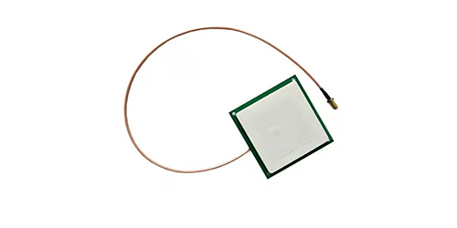
Another defining feature of SMD GPS antennas is their integration with other electronic components on PCBs. This integration not only saves space but also improves signal integrity by minimizing the length of signal paths between the antenna and the GPS receiver chip. Shorter signal paths reduce signal loss and interference, which is critical for maintaining high positioning accuracy, especially in urban canyons or indoor environments where GPS signals are often weak or reflected. Many SMD GPS antennas also include built-in matching networks, which optimize the impedance between the antenna and the receiver to ensure maximum power transfer. This integration simplifies the design process for engineers, as they do not need to design separate matching circuits, reducing time-to-market for new devices.
In terms of market adoption, SMD GPS antennas have become the standard choice for most compact electronics. According to industry reports, the global SMD antenna market is projected to grow at a compound annual growth rate (CAGR) of over 8% from 2024 to 2030, driven by the proliferation of IoT devices, wearables, and smart automotive systems. Key manufacturers, such as Taoglas, Johanson Technology, and Kyocera, offer a wide range of SMD GPS antenna models tailored to different applications, with variations in size, gain, radiation pattern, and environmental resistance. For example, some antennas are designed to be waterproof or dustproof (meeting IP67 or IP68 standards) for use in outdoor or rugged environments, while others prioritize ultra-low power consumption for battery-powered devices like fitness trackers.
It is also important to note that SMD GPS antennas are not a one-size-fits-all solution. Their performance depends on several factors, including the antenna’s design, the surrounding PCB layout, and the operating environment. For instance, metal components near the antenna can block or reflect GPS signals, reducing accuracy. As a result, engineers must carefully consider the placement of SMD GPS antennas on PCBs, often placing them at the edge of the board or in areas with minimal metal interference. Additionally, the choice between passive and active SMD GPS antennas depends on the application: passive antennas are simpler and more cost-effective but require a strong GPS signal, while active antennas include a low-noise amplifier (LNA) to boost weak signals, making them suitable for environments with poor signal reception.
In summary, SMD GPS antennas are a cornerstone of modern compact electronics, enabling accurate positioning in devices where space and weight are critical constraints. Their small form factor, easy integration with PCBs, and compatibility with multiple satellite constellations make them versatile for a wide range of applications, from consumer wearables to industrial IoT and automotive systems. As technology continues to advance, SMD GPS antennas will likely become even smaller, more efficient, and more resilient, further expanding their role in the growing ecosystem of location-enabled devices.
The design and construction of SMD GPS antennas are meticulously engineered to balance three core requirements: small form factor, high signal reception performance, and seamless integration with compact electronic devices. Unlike traditional external GPS antennas, which can afford larger sizes and simpler designs, SMD GPS antennas must operate within the tight space constraints of PCBs while maintaining the sensitivity needed to capture weak satellite signals. This section delves into the key design principles, materials, and construction techniques that define effective SMD GPS antennas, as well as the critical considerations that engineers must address to optimize their performance.
Core Design Principles
At the heart of SMD GPS antenna design is the need to resonate efficiently at the GPS L1 frequency (1575.42 MHz) (and often other satellite constellation frequencies, such as GLONASS’s L1 band at 1602 MHz or Galileo’s E1 band at 1575.42 MHz). Resonance is achieved by shaping the antenna’s radiating element to a specific length—typically a quarter-wavelength (λ/4) of the target frequency. For the L1 band, a quarter-wavelength is approximately 47 mm in free space, but since SMD antennas are mounted on PCBs (which have a higher dielectric constant than air), this length is shortened to around 10–15 mm. This miniaturization is critical for fitting the antenna into compact devices.
Another key design principle is impedance matching. GPS receivers typically have an input impedance of 50 ohms, so the antenna must be designed to match this impedance to ensure maximum power transfer and minimize signal loss. Most SMD GPS antennas include an integrated matching network, consisting of small capacitors and inductors, which is printed directly onto the antenna’s substrate or the PCB. This integration eliminates the need for external matching components, saving space and simplifying the design process.
Radiation pattern is also a critical design consideration. GPS antennas require an omnidirectional radiation pattern in the horizontal plane (azimuth) to receive signals from satellites in any part of the sky, while also having sufficient gain in the vertical plane (elevation) to capture signals from low-lying satellites. However, due to their small size, SMD GPS antennas often have a more directional pattern than larger external antennas, which can limit their performance in environments where satellites are low on the horizon (e.g., urban canyons). To mitigate this, some designs use a “patch” structure with a ground plane beneath the radiating element, which helps to focus the antenna’s radiation upward toward the sky, improving signal reception from overhead satellites.
Materials Selection
The choice of materials in SMD GPS antenna construction directly impacts performance, durability, and cost. The primary materials used include the substrate, radiating element, ground plane, and protective coating.
Substrate: The substrate is the base material onto which the radiating element and matching network are printed. It must have a stable dielectric constant (εr) and low loss tangent (tanδ) to minimize signal attenuation. Common substrates include FR-4 (a glass-reinforced epoxy resin, εr ≈ 4.4), Rogers 4350 (a high-performance laminate, εr ≈ 3.48), and ceramic materials (εr ≈ 9–12). FR-4 is cost-effective and widely used in consumer electronics, while Rogers 4350 and ceramics offer lower loss and better stability at high frequencies, making them suitable for high-precision applications like automotive ADAS or industrial IoT. The thickness of the substrate also affects performance: thinner substrates (0.2–0.5 mm) are preferred for compact devices, but thicker substrates can improve impedance matching and gain.
Radiating Element: The radiating element is the part of the antenna that captures GPS signals. It is typically made of a thin layer of copper (5–10 μm thick) printed onto the substrate using photolithography—a process that allows for precise patterning of the element’s shape (e.g., rectangular patch, meandered line, or spiral). Copper is ideal because it has high electrical conductivity, which minimizes resistive loss, and is compatible with standard PCB manufacturing processes. Some advanced designs use silver or gold plating for the radiating element to further reduce loss, though this increases cost and is typically reserved for high-end applications.
Ground Plane: The ground plane is a conductive layer (usually copper) located beneath the substrate, opposite the radiating element. It serves two key purposes: it acts as a reference for the antenna’s electrical field, and it blocks interference from other components on the PCB (e.g., microprocessors, power supplies) that could disrupt GPS signals. The size and shape of the ground plane are critical—too small, and the antenna’s radiation pattern becomes distorted; too large, and it takes up valuable space on the PCB. For SMD GPS antennas, the ground plane is often integrated into the PCB’s ground layer, with a minimum size of 10 mm × 10 mm to ensure stable performance.
Protective Coating: To protect the antenna from environmental damage (e.g., moisture, dust, or mechanical stress), a thin protective coating is applied over the radiating element. Common coatings include epoxy resins, polyimide films, or solder masks (the same material used to protect other parts of the PCB). For rugged applications (e.g., outdoor IoT sensors), the antenna may be encapsulated in a waterproof material like PTFE or silicone, meeting IP67 or IP68 standards. The coating must be thin (typically 10–50 μm) and have a low dielectric constant to avoid altering the antenna’s resonance frequency.
Construction Techniques
SMD GPS antennas are manufactured using standard PCB assembly processes, which ensures compatibility with high-volume production. The key steps in their construction include:
Substrate Preparation: The chosen substrate (e.g., FR-4 or Rogers 4350) is cut to the desired size (often as small as 2 mm × 2 mm for ultra-compact antennas) and cleaned to remove any contaminants that could affect signal performance.
Radiating Element and Matching Network Patterning: A thin layer of copper is laminated onto the top surface of the substrate. Using photolithography, the copper is etched into the precise shape of the radiating element and matching network. This process involves applying a photoresist layer, exposing it to a pattern of light (using a mask), developing the resist, and then etching away the unwanted copper. The result is a high-precision, low-loss conductive pattern.
Ground Plane Integration: If the ground plane is not part of the PCB’s existing ground layer, a copper layer is laminated onto the bottom surface of the substrate and connected to the PCB’s ground via vias (small holes drilled through the substrate and plated with copper). This ensures a low-impedance connection between the antenna’s ground plane and the rest of the device’s ground system, reducing noise and interference.
Component Mounting (for Active Antennas): Active SMD GPS antennas require an LNA to boost weak signals. The LNA, along with any other active components (e.g., voltage regulators), is mounted onto the substrate using SMD soldering techniques—either through reflow soldering (where the substrate is heated to melt solder paste applied to the component pads) or wave soldering (for high-volume production). The LNA is typically placed as close as possible to the radiating element to minimize signal loss between the antenna and the amplifier.
Testing and Calibration: After construction, each SMD GPS antenna undergoes rigorous testing to ensure it meets performance specifications. Key tests include measuring resonance frequency (using a network analyzer to check S11 parameter, which indicates how much signal is reflected back from the antenna), gain (using an anechoic chamber to measure the antenna’s ability to capture signals), and noise figure (for active antennas, to ensure the LNA does not introduce excessive noise). Antennas that do not meet specifications are calibrated—for example, by adjusting the size of the radiating element or the values of the matching network components—before being approved for use.
Critical Design Considerations
Engineers face several challenges when designing SMD GPS antennas for compact electronics, and addressing these is essential for optimal performance:
PCB Layout Interference: Metal components (e.g., batteries, speakers, or other antennas) near the SMD GPS antenna can block or reflect GPS signals, reducing accuracy. To mitigate this, engineers often place the antenna at the edge of the PCB, away from metal components, and use a “clearance area” (a region around the antenna with no metal) of at least 5 mm × 5 mm. Additionally, high-speed digital signals from microprocessors can generate electromagnetic interference (EMI) that disrupts GPS signals, so the antenna should be isolated from digital circuits using ground planes or shielding.
Environmental Factors: Temperature, humidity, and mechanical stress can affect the antenna’s performance. For example, changes in temperature can cause the substrate to expand or contract, altering the resonance frequency. To address this, engineers use substrates with low thermal expansion coefficients (e.g., ceramics) and design the radiating element to be resilient to temperature changes. For outdoor applications, waterproof coatings and ruggedized enclosures protect the antenna from moisture and physical damage.
Power Consumption (for Active Antennas): Battery-powered devices like wearables require active SMD GPS antennas with low power consumption. Engineers optimize the LNA’s design to operate at low voltages (typically 1.8–3.3 V) and low currents (10–30 mA), while still providing sufficient gain (15–25 dB) to boost weak signals. Some advanced designs also include power-saving modes, where the LNA is turned off when not in use, extending battery life.
In conclusion, the design and construction of SMD GPS antennas are a complex interplay of material science, electromagnetic engineering, and manufacturing technology. By focusing on miniaturization, impedance matching, and integration with PCBs, these antennas meet the demands of compact electronics while delivering the high performance needed for accurate GPS positioning. As devices continue to shrink and require more advanced location-based features, the design of SMD GPS antennas will evolve further, with innovations in materials (e.g., flexible substrates for foldable devices) and manufacturing techniques (e.g., 3D printing for complex shapes) driving even greater efficiency and versatility.
To understand how SMD GPS antennas enable accurate positioning in compact electronics, it is essential to explore their underlying working principles—from signal reception and conversion to integration with GPS receivers and the role of satellite constellations. Unlike larger external GPS antennas, SMD GPS antennas operate within the constraints of small form factors and PCB integration, but their core functionality remains rooted in fundamental electromagnetic principles. This section breaks down the key steps in the SMD GPS antenna’s operation, explains how it overcomes challenges like weak signals and interference, and highlights the differences between passive and active designs.
Step 1: Capturing GPS Satellite Signals
The primary function of any GPS antenna—including SMD models—is to capture electromagnetic signals transmitted by GPS satellites. GPS satellites orbit Earth at an altitude of approximately 20,200 km, in six orbital planes, ensuring that at least four satellites are visible from any point on the planet at any time (a requirement for accurate 3D positioning: latitude, longitude, and altitude). Each satellite transmits two types of signals in the L-band: the L1 signal (1575.42 MHz) for civilian use and the L2 signal (1227.60 MHz) for military and high-precision civilian applications. Most SMD GPS antennas are designed to receive the L1 signal, though advanced models may support L2 or signals from other constellations (GLONASS, Galileo, BeiDou) to improve reliability.
Electromagnetic signals from GPS satellites travel through the atmosphere (ionosphere and troposphere) before reaching the Earth’s surface. By the time these signals reach a compact device (e.g., a smartwatch), they are extremely weak—typically on the order of -130 dBm to -160 dBm (equivalent to a few picowatts). This weakness is one of the biggest challenges for SMD GPS antennas, as their small size limits their ability to capture signal energy. To address this, SMD GPS antennas are designed with a radiating element that resonates at the L1 frequency. Resonance occurs when the length of the radiating element is a multiple of the signal’s wavelength (usually a quarter-wavelength, λ/4), allowing the element to efficiently absorb the signal’s energy.
The radiating element of an SMD GPS antenna is typically a rectangular patch or meandered line printed on a substrate (e.g., FR-4 or ceramic). When a GPS signal reaches the radiating element, it induces an alternating electric current in the element. This current is generated because the electromagnetic signal’s electric field interacts with the conductive material of the radiating element, causing electrons to oscillate at the signal’s frequency (1575.42 MHz). The ground plane beneath the substrate plays a critical role here: it acts as a mirror for the electromagnetic field, focusing the antenna’s radiation upward toward the sky (where satellites are located) and preventing signal loss downward into the PCB.
Step 2: Converting Signals to Electrical Energy
Once the radiating element captures the GPS signal and induces an electric current, the next step is to convert this current into a usable electrical signal that can be processed by the GPS receiver. This conversion isfacilitated by the antenna’s integrated matching network, which plays a pivotal role in optimizing signal transfer. As mentioned earlier, GPS receivers typically have an input impedance of 50 ohms, and any mismatch between the antenna’s impedance and the receiver’s impedance would result in signal reflection—meaning a portion of the induced current is bounced back instead of being transmitted to the receiver. The matching network, composed of small capacitors and inductors printed on the substrate, adjusts the antenna’s impedance to match the receiver’s 50-ohm requirement. This ensures maximum power transfer, minimizing signal loss and preserving the weak GPS signal’s integrity.
For passive SMD GPS antennas, the converted electrical signal is sent directly to the GPS receiver via a short coaxial cable or a PCB trace. However, given the extremely low power of GPS signals (often below the receiver’s minimum detectable threshold), passive antennas are only effective in environments with strong signal reception—such as open outdoor spaces with unobstructed views of the sky. In contrast, active SMD GPS antennas address the signal weakness by incorporating a low-noise amplifier (LNA) immediately after the radiating element. The LNA boosts the electrical signal by 15–25 dB (a 30–300x increase in power) while introducing minimal additional noise. This is critical because any noise added by the amplifier could obscure the weak GPS signal, so LNAs are designed with a low noise figure (typically 1–2 dB) to ensure the amplified signal remains clean and usable.
The LNA’s placement is strategic: it is mounted as close as possible to the radiating element—often directly on the antenna’s substrate—to minimize signal loss before amplification. If the LNA were placed further away (e.g., on the opposite side of the PCB), the weak signal would degrade as it travels through the PCB trace, and amplifying a degraded signal would only magnify the loss and noise, reducing overall performance. By integrating the LNA into the antenna module, active SMD GPS antennas ensure that the signal is boosted at the earliest possible stage, preserving its quality for subsequent processing.
Step 3: Signal Processing by the GPS Receiver
Once the SMD GPS antenna delivers the amplified (or passive) electrical signal to the GPS receiver, the receiver takes over to extract location data. The receiver’s first task is to downconvert the high-frequency L1 signal (1575.42 MHz) to a lower intermediate frequency (IF), typically a few megahertz. This downconversion simplifies subsequent processing, as lower-frequency signals are easier to filter and digitize. The receiver uses a local oscillator (LO) to generate a signal close to the L1 frequency; when mixed with the incoming GPS signal, this produces the IF signal.
Next, the receiver filters the IF signal to remove unwanted noise and interference—such as signals from other wireless devices (e.g., Wi-Fi, Bluetooth) operating in nearby frequency bands. This filtering is critical because compact electronics often contain multiple wireless components, and cross-interference can disrupt the GPS signal. The filtered IF signal is then digitized by an analog-to-digital converter (ADC), which converts the continuous analog signal into discrete digital data that can be processed by a microprocessor.
The core of the receiver’s processing is to decode the GPS signal’s data content. Each GPS satellite transmits two types of data: the C/A (Coarse/Acquisition) code and the navigation message. The C/A code is a pseudorandom noise (PRN) sequence—a unique 1023-bit pattern that identifies each satellite. The receiver uses a correlator to match the incoming C/A code with a locally generated PRN sequence. When the two sequences align (a process called “acquisition”), the receiver can determine the time delay between the satellite’s transmission and the signal’s arrival at the antenna. This time delay, known as the pseudorange, is the key to calculating distance: since the GPS signal travels at the speed of light (3×10⁸ m/s), the distance to the satellite is the pseudorange multiplied by the speed of light (adjusted for delays caused by the atmosphere and receiver clock errors).
The navigation message, transmitted at a much slower rate (50 bits per second), contains critical information about the satellite’s orbit (ephemeris data), the health of the satellite, and the time of transmission (clock data). The receiver uses the ephemeris data to determine the satellite’s exact position in space at the time of transmission. With pseudoranges to at least four satellites and their known positions, the receiver can solve a system of equations to calculate the device’s 3D location (latitude, longitude, altitude) using a process called trilateration.
Step 4: Overcoming Environmental Challenges
SMD GPS antennas face unique challenges in compact electronics, particularly related to signal blockage and interference. The antenna’s small size and integration into PCBs mean it is often surrounded by metal components (e.g., batteries, speakers, display modules) and other wireless antennas, which can block or reflect GPS signals. To mitigate this, the antenna’s design and placement are optimized to minimize obstruction. For example, the ground plane beneath the radiating element not only enhances upward radiation but also acts as a shield against electromagnetic interference (EMI) from components below the PCB. Additionally, engineers often place the SMD GPS antenna at the edge of the PCB, where it has a clearer line of sight to the sky and is farther from metal components.
Another challenge is signal degradation in urban or indoor environments. In urban canyons—areas with tall buildings—GPS signals are reflected off buildings and other surfaces, creating multipath interference. This causes the receiver to measure incorrect pseudoranges, leading to location errors. Some advanced SMD GPS antennas address this by using beamforming technology, which focuses the antenna’s radiation pattern to prioritize direct signals over reflected ones. However, beamforming is more common in larger antennas; for SMD models, manufacturers often rely on multi-constellation support (e.g., combining GPS with GLONASS or Galileo) to increase the number of visible satellites, reducing the impact of multipath by providing more redundant pseudorange data.
Indoor environments pose an even greater challenge, as GPS signals are heavily attenuated by walls, roofs, and other structures. In these cases, active SMD GPS antennas with high-gain LNAs (25–30 dB) can help capture weak indoor signals, but performance is still limited. To improve indoor positioning, some devices combine SMD GPS antennas with other technologies like Wi-Fi fingerprinting or Bluetooth beacons, creating a hybrid positioning system that leverages GPS for outdoor accuracy and alternative signals for indoor coverage.
Passive vs. Active SMD GPS Antennas: Key Operational Differences
The working principles of SMD GPS antennas vary slightly between passive and active designs, and understanding these differences is critical for selecting the right antenna for an application:
Passive Antennas: These antennas lack an LNA, so they rely solely on the radiating element and matching network to deliver signals to the receiver. Their operation is simpler: the radiating element captures the GPS signal, the matching network optimizes impedance, and the signal is sent directly to the receiver. Passive antennas are smaller, lighter, and more cost-effective than active models, and they consume no power—making them ideal for battery-powered devices where power efficiency is paramount (e.g., low-cost IoT sensors). However, their performance is limited to strong signal environments; in urban or indoor settings, the weak signal may be too faint for the receiver to detect, leading to positioning errors or loss of signal.
Active Antennas: These antennas include an LNA, which amplifies the signal before it reaches the receiver. The LNA’s low noise figure ensures that the amplified signal retains its integrity, even in weak signal environments. Active antennas are more complex than passive ones, as they require a power source (typically 1.8–3.3 V from the device’s battery) to operate the LNA. They also consume more power (10–30 mA) and are slightly larger due to the LNA component. However, their ability to boost weak signals makes them the preferred choice for devices used in urban canyons, indoor spaces, or other challenging environments (e.g., automotive ADAS, high-precision wearables). Many active SMD GPS antennas also include a voltage regulator to stabilize the power supply to the LNA, ensuring consistent performance even if the device’s battery voltage fluctuates.
Conclusion of Working Principles
The working principles of SMD GPS antennas are a testament to the engineering innovations that enable accurate positioning in compact electronics. From the radiating element’s resonance at the L1 frequency to the LNA’s signal amplification and the receiver’s trilateration calculations, every step is optimized to overcome the challenges of small form factors and weak satellite signals. Passive antennas excel in power efficiency and simplicity, while active antennas deliver the performance needed for demanding environments. By integrating these principles with careful PCB design and environmental mitigation strategies, SMD GPS antennas ensure that even the smallest devices—from smartwatches to IoT sensors—can reliably access location data, powering the growing ecosystem of location-based services.
SMD GPS antennas have revolutionized the design of compact electronic devices by enabling precise positioning in space-constrained form factors. However, like any technology, they come with a unique set of advantages that drive their adoption and challenges that engineers must address to maximize their performance. This section explores these advantages in detail, from space efficiency to cost-effectiveness, and examines the key challenges—such as signal interference and environmental sensitivity—along with strategies to mitigate them.
Core Advantages of SMD GPS Antennas
1. Ultra-Compact Size and Low Profile
The most defining advantage of SMD GPS antennas is their small form factor, which aligns perfectly with the trend toward miniaturization in electronics. Traditional external GPS antennas often require bulky enclosures and mounting hardware, taking up valuable space in devices like smartwatches or IoT sensors. In contrast, SMD GPS antennas are designed to be soldered directly onto PCBs, with typical dimensions ranging from 2 mm × 2 mm × 1 mm to 10 mm × 10 mm × 5 mm. This ultra-compact size allows them to fit into even the smallest devices—such as fitness trackers, smart rings, or miniaturized industrial sensors—without compromising the device’s sleek design or functionality.
Their low profile (1–5 mm in height) is another critical benefit. In devices where thickness is a priority (e.g., slim smartphones, foldable tablets), a low-profile antenna avoids adding bulk, ensuring the device remains portable and aesthetically pleasing. This is in stark contrast to through-hole GPS antennas, which often protrude from the PCB, limiting their use in thin devices.
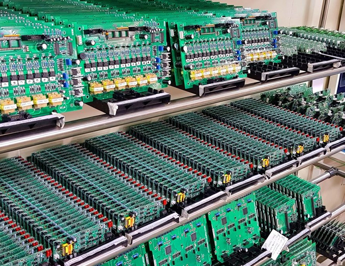
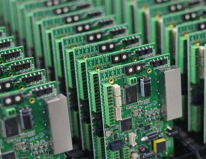
2. Seamless PCB Integration and Simplified Manufacturing
SMD GPS antennas leverage surface-mount technology (SMT), which is the standard for modern PCB assembly. This means they can be integrated into the same manufacturing process as other SMD components (e.g., microchips, resistors, capacitors), eliminating the need for separate assembly steps. During production, SMD GPS antennas are placed on the PCB using automated pick-and-place machines and soldered via reflow soldering—a high-volume, cost-effective process that ensures consistent quality.
This integration also simplifies the design process for engineers. Unlike external antennas, which require wiring, connectors, and mounting brackets, SMD GPS antennas are directly connected to the PCB via solder pads. This reduces the number of components needed, streamlines the PCB layout, and shortens the signal path between the antenna and the GPS receiver. Shorter signal paths minimize signal loss and interference, improving overall positioning accuracy—a critical advantage in weak signal environments.
3. Cost-Effectiveness for Mass Production
SMD GPS antennas are highly cost-effective for mass-produced devices, thanks to their compatibility with automated manufacturing processes. The use of standard SMT equipment reduces labor costs, as there is no need for manual installation of external antennas. Additionally, the materials used in SMD GPS antennas—such as FR-4 substrates and copper radiating elements—are relatively inexpensive compared to the materials required for external antennas (e.g., plastic enclosures, coaxial cables).
For high-volume applications (e.g., smartphones, consumer wearables), manufacturers can also benefit from economies of scale. As production volumes increase, the cost per unit of SMD GPS antennas decreases, making them more affordable than traditional alternatives. Even active SMD GPS antennas— which include an LNA—are cost-competitive, as the LNA is a small, mass-produced component that adds minimal cost to the antenna module.
4. Versatility Across Applications
SMD GPS antennas are highly versatile, with designs tailored to meet the needs of diverse applications. Manufacturers offer a wide range of models with variations in size, gain, radiation pattern, and environmental resistance, allowing engineers to select the right antenna for their specific use case:
Consumer Electronics: For devices like smartwatches or fitness trackers, ultra-small SMD GPS antennas (2 mm × 2 mm) with low power consumption are ideal. These antennas prioritize size and battery efficiency over high gain, as they are typically used in outdoor environments with strong signal reception.
Automotive Systems: Automotive-grade SMD GPS antennas are designed to withstand harsh conditions, including extreme temperatures (-40°C to 85°C), vibration, and moisture. They often include high-gain LNAs to ensure reliable performance in urban canyons or under vehicle roofs, supporting applications like in-car navigation and ADAS.
Industrial IoT: Industrial SMD GPS antennas may be ruggedized to meet IP67 or IP68 standards (waterproof and dustproof) for use in outdoor or harsh industrial environments (e.g., construction sites, oil rigs). They may also support multi-constellation reception (GPS, GLONASS, Galileo) to improve accuracy in remote areas.
Medical Devices: For portable medical devices (e.g., patient trackers), SMD GPS antennas are designed to be lightweight and biocompatible, with low power consumption to extend battery life.
5. Improved Signal Integrity and Reduced Interference
The integration of SMD GPS antennas into PCBs—along with built-in matching networks—improves signal integrity by minimizing signal loss and interference. The short signal path between the antenna and the receiver reduces attenuation, ensuring that more of the weak GPS signal reaches the receiver. The matching network optimizes impedance, preventing signal reflection and maximizing power transfer.
Additionally, the ground plane beneath the SMD GPS antenna’s radiating element acts as a shield against EMI from other components on the PCB. High-speed digital circuits (e.g., microprocessors, memory chips) generate electromagnetic noise that can disrupt GPS signals, but the ground plane blocks this noise from reaching the radiating element. This is particularly important in compact devices, where components are densely packed and EMI risks are higher.
Key Challenges of SMD GPS Antennas
1. Signal Blockage and Interference from PCB Components
The biggest challenge facing SMD GPS antennas is signal blockage and interference from other components on the PCB. Compact devices often have limited space, so the antenna is frequently placed near metal components—such as batteries, speakers, display modules, or other wireless antennas (Wi-Fi, Bluetooth). Metal reflects GPS signals, which can block the antenna’s line of sight to satellites and create multipath interference. For example, a battery placed directly above the SMD GPS antenna can block up to 50% of the signal, leading to reduced accuracy or loss of signal.
High-speed digital components also generate EMI that can disrupt the weak GPS signal. Even small amounts of noise—from a microprocessor’s clock signal, for example—can obscure the GPS signal, making it difficult for the receiver to decode the C/A code and navigation message. This is especially problematic in devices with multiple wireless radios, where cross-interference between GPS and other signals (e.g., 5G, Wi-Fi 6) can further degrade performance.
Mitigation Strategies:
Strategic PCB Placement: Engineers place the SMD GPS antenna at the edge of the PCB, where it has a clearer line of sight to the sky and is farther from metal components. They also define a “clearance area” (typically 5 mm × 5 mm) around the antenna where no metal components or high-speed traces are placed.
Ground Plane Shielding: A larger ground plane beneath the antenna can enhance shielding against EMI. Some designs use a “ground fence”—a ring of ground vias around the antenna—to isolate it from nearby digital circuits.
Filtering and Isolation: The GPS receiver’s input circuit may include a band-pass filter to block signals outside the L1 band, reducing interference from other wireless devices. Additionally, the antenna’s power supply (for active models) may include a low-pass filter to eliminate noise from the device’s power management system.
2. Limited Gain and Radiation Pattern Constraints
SMD GPS antennas have smaller radiating elements than external antennas, which limits their gain—the measure of the antenna’s ability to capture signal energy. Typical gain for a passive SMD GPS antenna is 0–2 dBi, while active models offer 15–25 dB (including the LNA’s gain). In comparison, external GPS antennas can have gains of 5–10 dBi or higher, making them more effective at capturing weak signals.
The small size also restricts the antenna’s radiation pattern. GPS antennas require an omnidirectional pattern in the azimuth plane to receive signals from satellites in any direction, but SMD models often have a more directional pattern—with reduced gain at low elevations (e.g., satellites near the horizon). This can limit performance in urban canyons, where satellites are often low on the horizon and signals are already weak.
Mitigation Strategies:
Multi-Constellation Support: By supporting multiple satellite constellations (GPS, GLONASS, Galileo, BeiDou), SMD GPS antennas increase the number of visible satellites. This provides more redundant pseudorange data, compensating for the antenna’s lower gain and improving accuracy.
Beamforming (Advanced Models): Some high-end SMD GPS antennas use beamforming technology, which adjusts the radiation pattern to focus on satellites with the strongest signals. While beamforming adds complexity and cost, it can significantly improve gain at low elevations.
Active LNAs with Higher Gain: For applications requiring stronger signal reception, active SMD GPS antennas with higher-gain LNAs (25–30 dB) can be used. These LNAs are designed with ultra-low noise figures (1 dB or less) to ensure the amplified signal remains clean.
3. Environmental Sensitivity
SMD GPS antennas are sensitive to environmental factors like temperature, humidity, and mechanical stress, which can alter their performance over time.
Temperature: Changes inManufacturers will develop antennas that can withstand extreme temperatures (ranging from -60°C for Arctic industrial sensors to 125°C for automotive under-hood applications), high pressure (for deep-sea IoT devices), and chemical exposure (for oil and gas industry sensors).
To achieve this, advanced materials will be adopted: for example, using ceramic-polymer composites for substrates, which combine the low thermal expansion of ceramics with the flexibility of polymers, ensuring the antenna remains stable in temperature fluctuations. For chemical resistance, the protective coating will be made of fluoropolymers (e.g., PFA) or ceramic enamels, which are impervious to corrosive substances like oil, solvents, and saltwater.
In addition, hermetic sealing techniques—such as laser welding or glass-to-metal sealing—will be used to create a fully airtight enclosure around the antenna, preventing moisture, dust, or gases from entering. This is particularly critical for deep-sea devices, where high pressure can force moisture into even the smallest gaps, and for medical implants, where hermetic sealing ensures biocompatibility and prevents infection.
6. Integration with 5G and V2X Technologies
As 5G networks become more widespread and vehicle-to-everything (V2X) communication emerges as a key enabler of autonomous driving, SMD GPS antennas will be increasingly integrated with 5G and V2X antennas into a single “multi-functional antenna module.” This integration will reduce the overall size and cost of the device’s wireless system, while also improving coordination between positioning and communication.
For example, in autonomous vehicles, the integrated module will use the SMD GPS antenna for precise positioning and the 5G/V2X antenna to communicate with other vehicles, infrastructure, and the cloud. The module will share a common ground plane and signal processing unit, minimizing interference and ensuring real-time synchronization between positioning data and communication signals. This integration will be critical for autonomous driving, where even a small delay between positioning and communication could lead to safety risks.
Conclusion of Applications and Future Trends
SMD GPS antennas have already transformed the landscape of compact electronics, enabling location-based functionality in devices that were once too small or power-constrained for traditional GPS antennas. Their applications span consumer wearables, IoT, automotive, medical, and consumer electronics—each leveraging the antenna’s compact size, seamless integration, and versatility to deliver innovative features.
Looking ahead, the future of SMD GPS antennas is defined by continuous innovation: further miniaturization will unlock new applications in micro-IoT and implantable devices; enhanced multi-constellation and multi-band support will deliver sub-meter accuracy; AI integration will optimize performance in dynamic environments; reduced power consumption and energy harvesting will extend battery life; improved ruggedness will enable use in extreme conditions; and integration with 5G/V2X will support the next generation of connected and autonomous systems.
As these trends unfold, SMD GPS antennas will remain a critical component in the growing ecosystem of location-enabled devices, driving progress in industries from healthcare to automotive and shaping the way we interact with technology in our daily lives.
SMD GPS antennas have revolutionized the design of compact electronic devices by enabling precise positioning in space-constrained form factors. However, like any technology, they come with a unique set of advantages that drive their adoption and challenges that engineers must address to maximize their performance. This section explores these advantages in detail, from space efficiency to cost-effectiveness, and examines the key challenges—such as signal interference and environmental sensitivity—along with strategies to mitigate them.
Core Advantages of SMD GPS Antennas
1. Ultra-Compact Size and Low Profile
The most defining advantage of SMD GPS antennas is their small form factor, which aligns perfectly with the trend toward miniaturization in electronics. Traditional external GPS antennas often require bulky enclosures and mounting hardware, taking up valuable space in devices like smartwatches or IoT sensors. In contrast, SMD GPS antennas are designed to be soldered directly onto PCBs, with typical dimensions ranging from 2 mm × 2 mm × 1 mm to 10 mm × 10 mm × 5 mm. This ultra-compact size allows them to fit into even the smallest devices—such as fitness trackers, smart rings, or miniaturized industrial sensors—without compromising the device’s sleek design or functionality.
Their low profile (1–5 mm in height) is another critical benefit. In devices where thickness is a priority (e.g., slim smartphones, foldable tablets), a low-profile antenna avoids adding bulk, ensuring the device remains portable and aesthetically pleasing. This is in stark contrast to through-hole GPS antennas, which often protrude from the PCB, limiting their use in thin devices.
2. Seamless PCB Integration and Simplified Manufacturing
SMD GPS antennas leverage surface-mount technology (SMT), which is the standard for modern PCB assembly. This means they can be integrated into the same manufacturing process as other SMD components (e.g., microchips, resistors, capacitors), eliminating the need for separate assembly steps. During production, SMD GPS antennas are placed on the PCB using automated pick-and-place machines and soldered via reflow soldering—a high-volume, cost-effective process that ensures consistent quality.
This integration also simplifies the design process for engineers. Unlike external antennas, which require wiring, connectors, and mounting brackets, SMD GPS antennas are directly connected to the PCB via solder pads. This reduces the number of components needed, streamlines the PCB layout, and shortens the signal path between the antenna and the GPS receiver. Shorter signal paths minimize signal loss and interference, improving overall positioning accuracy—a critical advantage in weak signal environments.
3. Cost-Effectiveness for Mass Production
SMD GPS antennas are highly cost-effective for mass-produced devices, thanks to their compatibility with automated manufacturing processes. The use of standard SMT equipment reduces labor costs, as there is no need for manual installation of external antennas. Additionally, the materials used in SMD GPS antennas—such as FR-4 substrates and copper radiating elements—are relatively inexpensive compared to the materials required for external antennas (e.g., plastic enclosures, coaxial cables).
For high-volume applications (e.g., smartphones, consumer wearables), manufacturers can also benefit from economies of scale. As production volumes increase, the cost per unit of SMD GPS antennas decreases, making them more affordable than traditional alternatives. Even active SMD GPS antennas— which include an LNA—are cost-competitive, as the LNA is a small, mass-produced component that adds minimal cost to the antenna module.
4. Versatility Across Applications
SMD GPS antennas are highly versatile, with designs tailored to meet the needs of diverse applications. Manufacturers offer a wide range of models with variations in size, gain, radiation pattern, and environmental resistance, allowing engineers to select the right antenna for their specific use case:
Consumer Electronics: For devices like smartwatches or fitness trackers, ultra-small SMD GPS antennas (2 mm × 2 mm) with low power consumption are ideal. These antennas prioritize size and battery efficiency over high gain, as they are typically used in outdoor environments with strong signal reception.
Automotive Systems: Automotive-grade SMD GPS antennas are designed to withstand harsh conditions, including extreme temperatures (-40°C to 85°C), vibration, and moisture. They often include high-gain LNAs to ensure reliable performance in urban canyons or under vehicle roofs, supporting applications like in-car navigation and ADAS.
Industrial IoT: Industrial SMD GPS antennas may be ruggedized to meet IP67 or IP68 standards (waterproof and dustproof) for use in outdoor or harsh industrial environments (e.g., construction sites, oil rigs). They may also support multi-constellation reception (GPS, GLONASS, Galileo) to improve accuracy in remote areas.
Medical Devices: For portable medical devices (e.g., patient trackers), SMD GPS antennas are designed to be lightweight and biocompatible, with low power consumption to extend battery life.
5. Improved Signal Integrity and Reduced Interference
The integration of SMD GPS antennas into PCBs—along with built-in matching networks—improves signal integrity by minimizing signal loss and interference. The short signal path between the antenna and the receiver reduces attenuation, ensuring that more of the weak GPS signal reaches the receiver. The matching network optimizes impedance, preventing signal reflection and maximizing power transfer.
Additionally, the ground plane beneath the SMD GPS antenna’s radiating element acts as a shield against EMI from other components on the PCB. High-speed digital circuits (e.g., microprocessors, memory chips) generate electromagnetic noise that can disrupt GPS signals, but the ground plane blocks this noise from reaching the radiating element. This is particularly important in compact devices, where components are densely packed and EMI risks are higher.
Key Challenges of SMD GPS Antennas
1. Signal Blockage and Interference from PCB Components
The biggest challenge facing SMD GPS antennas is signal blockage and interference from other components on the PCB. Compact devices often have limited space, so the antenna is frequently placed near metal components—such as batteries, speakers, display modules, or other wireless antennas (Wi-Fi, Bluetooth). Metal reflects GPS signals, which can block the antenna’s line of sight to satellites and create multipath interference. For example, a battery placed directly above the SMD GPS antenna can block up to 50% of the signal, leading to reduced accuracy or loss of signal.
High-speed digital components also generate EMI that can disrupt the weak GPS signal. Even small amounts of noise—from a microprocessor’s clock signal, for example—can obscure the GPS signal, making it difficult for the receiver to decode the C/A code and navigation message. This is especially problematic in devices with multiple wireless radios, where cross-interference between GPS and other signals (e.g., 5G, Wi-Fi 6) can further degrade performance.
Mitigation Strategies:
Strategic PCB Placement: Engineers place the SMD GPS antenna at the edge of the PCB, where it has a clearer line of sight to the sky and is farther from metal components. They also define a “clearance area” (typically 5 mm × 5 mm) around the antenna where no metal components or high-speed traces are placed.
Ground Plane Shielding: A larger ground plane beneath the antenna can enhance shielding against EMI. Some designs use a “ground fence”—a ring of ground vias around the antenna—to isolate it from nearby digital circuits.
Filtering and Isolation: The GPS receiver’s input circuit may include a band-pass filter to block signals outside the L1 band, reducing interference from other wireless devices. Additionally, the antenna’s power supply (for active models) may include a low-pass filter to eliminate noise from the device’s power management system.
2. Limited Gain and Radiation Pattern Constraints
SMD GPS antennas have smaller radiating elements than external antennas, which limits their gain—the measure of the antenna’s ability to capture signal energy. Typical gain for a passive SMD GPS antenna is 0–2 dBi, while active models offer 15–25 dB (including the LNA’s gain). In comparison, external GPS antennas can have gains of 5–10 dBi or higher, making them more effective at capturing weak signals.
The small size also restricts the antenna’s radiation pattern. GPS antennas require an omnidirectional pattern in the azimuth plane to receive signals from satellites in any direction, but SMD models often have a more directional pattern—with reduced gain at low elevations (e.g., satellites near the horizon). This can limit performance in urban canyons, where satellites are often low on the horizon and signals are already weak.
Mitigation Strategies:
Multi-Constellation Support: By supporting multiple satellite constellations (GPS, GLONASS, Galileo, BeiDou), SMD GPS antennas increase the number of visible satellites. This provides more redundant pseudorange data, compensating for the antenna’s lower gain and improving accuracy.
Beamforming (Advanced Models): Some high-end SMD GPS antennas use beamforming technology, which adjusts the radiation pattern to focus on satellites with the strongest signals. While beamforming adds complexity and cost, it can significantly improve gain at low elevations.
Active LNAs with Higher Gain: For applications requiring stronger signal reception, active SMD GPS antennas with higher-gain LNAs (25–30 dB) can be used. These LNAs are designed with ultra-low noise figures (1 dB or less) to ensure the amplified signal remains clean.
3. Environmental Sensitivity
SMD GPS antennas are sensitive to environmental factors like temperature, humidity, and mechanical stress, which can alter their performance over time.
Temperature: Changes inManufacturers will develop antennas that can withstand extreme temperatures (ranging from -60°C for Arctic industrial sensors to 125°C for automotive under-hood applications), high pressure (for deep-sea IoT devices), and chemical exposure (for oil and gas industry sensors).
To achieve this, advanced materials will be adopted: for example, using ceramic-polymer composites for substrates, which combine the low thermal expansion of ceramics with the flexibility of polymers, ensuring the antenna remains stable in temperature fluctuations. For chemical resistance, the protective coating will be made of fluoropolymers (e.g., PFA) or ceramic enamels, which are impervious to corrosive substances like oil, solvents, and saltwater.
In addition, hermetic sealing techniques—such as laser welding or glass-to-metal sealing—will be used to create a fully airtight enclosure around the antenna, preventing moisture, dust, or gases from entering. This is particularly critical for deep-sea devices, where high pressure can force moisture into even the smallest gaps, and for medical implants, where hermetic sealing ensures biocompatibility and prevents infection.
6. Integration with 5G and V2X Technologies
As 5G networks become more widespread and vehicle-to-everything (V2X) communication emerges as a key enabler of autonomous driving, SMD GPS antennas will be increasingly integrated with 5G and V2X antennas into a single “multi-functional antenna module.” This integration will reduce the overall size and cost of the device’s wireless system, while also improving coordination between positioning and communication.
For example, in autonomous vehicles, the integrated module will use the SMD GPS antenna for precise positioning and the 5G/V2X antenna to communicate with other vehicles, infrastructure, and the cloud. The module will share a common ground plane and signal processing unit, minimizing interference and ensuring real-time synchronization between positioning data and communication signals. This integration will be critical for autonomous driving, where even a small delay between positioning and communication could lead to safety risks.
Conclusion of Applications and Future Trends
SMD GPS antennas have already transformed the landscape of compact electronics, enabling location-based functionality in devices that were once too small or power-constrained for traditional GPS antennas. Their applications span consumer wearables, IoT, automotive, medical, and consumer electronics—each leveraging the antenna’s compact size, seamless integration, and versatility to deliver innovative features.
Looking ahead, the future of SMD GPS antennas is defined by continuous innovation: further miniaturization will unlock new applications in micro-IoT and implantable devices; enhanced multi-constellation and multi-band support will deliver sub-meter accuracy; AI integration will optimize performance in dynamic environments; reduced power consumption and energy harvesting will extend battery life; improved ruggedness will enable use in extreme conditions; and integration with 5G/V2X will support the next generation of connected and autonomous systems.
As these trends unfold, SMD GPS antennas will remain a critical component in the growing ecosystem of location-enabled devices, driving progress in industries from healthcare to automotive and shaping the way we interact with technology in our daily lives.
6. Conclusion: The Evolving Role of SMD GPS Antennas in Compact Electronics
Surface-Mount Device (SMD) GPS antennas have emerged as a transformative technology in the field of satellite positioning, addressing the core demands of modern compact electronics: space efficiency, seamless integration, and reliable performance. Over the years, they have evolved from niche components to indispensable building blocks, powering location-based services across consumer, industrial, automotive, and medical sectors. This conclusion synthesizes the key insights from the preceding sections, highlights the broader impact of SMD GPS antennas on technology innovation, and reflects on their long-term significance in an increasingly connected world.
A Synthesis of Core Strengths
At their essence, SMD GPS antennas excel in solving the “size-performance paradox” that has long challenged compact electronics. Traditional external GPS antennas, with their bulky enclosures and mounting hardware, could not keep pace with the trend toward miniaturization—whether in a 2 mm × 2 mm smart ring or a micro-IoT sensor deployed in a manufacturing facility. SMD GPS antennas resolve this by leveraging surface-mount technology, allowing direct soldering onto PCBs and eliminating the need for extra components. Their low profile (1–5 mm) and small form factor make them compatible with the slimmest devices, while integrated matching networks and (in active models) low-noise amplifiers (LNAs) ensure they deliver the sensitivity needed to capture weak GPS signals.
Cost-effectiveness is another core strength. By integrating into standard PCB assembly processes—using automated pick-and-place machines and reflow soldering—SMD GPS antennas reduce manufacturing complexity and labor costs. This has made them accessible to high-volume consumer devices (e.g., smartphones, fitness trackers) and low-cost IoT sensors alike, democratizing access to accurate positioning technology. For example, a budget-friendly fitness tracker can now include GPS functionality at a fraction of the cost of a device with a traditional external antenna, expanding the reach of location-based health and activity tracking.
Versatility further cements their value. SMD GPS antennas are not a one-size-fits-all solution; instead, they are tailored to diverse applications: passive models prioritize low power consumption for battery-powered wearables, active models with high-gain LNAs ensure reliability in urban canyons for automotive ADAS, and ruggedized models with IP67/IP68 ratings withstand harsh conditions for industrial IoT. This adaptability has allowed them to penetrate markets as varied as emergency medical services (where they enable fast patient location) and smart cities (where they power thousands of parking or waste management sensors).
Addressing Challenges: A Path of Continuous Improvement
While SMD GPS antennas offer significant advantages, they have not been without challenges— and the industry’s response to these challenges has been a driving force behind their evolution. Signal interference from nearby metal components or high-speed digital circuits, for instance, was once a major limitation. Today, engineers mitigate this through strategic PCB placement (e.g., edge positioning, 5 mm × 5 mm clearance areas), ground plane shielding, and band-pass filtering. Similarly, the limited gain of small radiating elements has been addressed by multi-constellation support (combining GPS, GLONASS, Galileo, and BeiDou) to increase the number of visible satellites, and by advanced LNAs with ultra-low noise figures to boost weak signals.
Environmental sensitivity—from temperature-induced frequency shifts to moisture damage—has also been tackled with material innovations: low-thermal-expansion substrates like Rogers 4350, waterproof PTFE coatings, and hermetic sealing for extreme conditions. Power consumption, a critical concern for battery-powered devices, has been reduced through low-power LNAs (consuming 5–10 mA) and power-saving modes (e.g., pulse mode, hybrid positioning with Wi-Fi/Bluetooth). These solutions not only overcome challenges but also push the boundaries of what SMD GPS antennas can achieve—turning limitations into opportunities for innovation.
Broader Impact on Technology and Society
The impact of SMD GPS antennas extends far beyond the components themselves; they have enabled a new generation of technology that reshapes how we live, work, and interact with the world. In consumer life, they have transformed wearables from simple activity trackers into comprehensive health monitors—allowing users to map their runs, track outdoor workouts, and even share their location in emergencies. In healthcare, they power patient trackers for individuals with dementia, ensuring caregivers can locate loved ones quickly, and enable remote health monitoring by tagging vital signs with location data (e.g., for patients traveling or living in rural areas).
In industry, SMD GPS antennas have revolutionized asset tracking—making it possible to monitor the location of shipping containers, industrial equipment, or even livestock with micro-IoT sensors. This has improved supply chain efficiency, reduced theft, and enabled real-time inventory management. In automotive, they are a cornerstone of advanced driver-assistance systems (ADAS) and autonomous driving, delivering the precise positioning needed for lane-keeping assist, adaptive cruise control, and V2X communication. For smart cities, they enable thousands of connected sensors to position themselves, creating intelligent infrastructure for parking, traffic management, and environmental monitoring—reducing congestion and improving quality of life.
The Road Ahead: A Future of Further Innovation
As we look to the future, the role of SMD GPS antennas will only grow in importance. The trends outlined earlier—ultra-miniaturization, AI integration, multi-constellation/multi-band support, energy harvesting, and 5G/V2X integration—will continue to drive their evolution. Ultra-miniature antennas (1 mm × 1 mm) will unlock applications in implantable medical devices (e.g., pacemakers with location tracking for emergency response) and micro-robots used in manufacturing or surgery. AI integration will enable dynamic performance optimization, with antennas adjusting their gain or radiation pattern in real time to adapt to urban canyons, remote areas, or indoor environments.
Energy harvesting—using solar cells or vibration harvesters—will make SMD GPS antennas self-sustaining, extending the lifespan of IoT sensors to 5–10 years and reducing the need for battery replacement in hard-to-reach locations. Integration with 5G and V2X will be critical for autonomous driving and smart infrastructure, ensuring seamless synchronization between positioning data and real-time communication. Together, these innovations will expand the capabilities of SMD GPS antennas, making them even more versatile and indispensable.
Final Reflections
SMD GPS antennas are more than just components; they are enablers of progress. They have turned the vision of “location in every device” into a reality, empowering developers to create products that are smaller, smarter, and more connected than ever before. Their journey from early prototypes to mass-produced essentials is a testament to the power of engineering innovation—solving complex challenges to meet the needs of a rapidly evolving technology landscape.
As compact electronics continue to penetrate every aspect of our lives—from the wearables on our wrists to the sensors powering our cities—SMD GPS antennas will remain at the forefront, driving innovation and shaping the future of location-based technology. Their legacy is not just in the devices they power, but in the way they have made accurate, reliable positioning accessible to all, opening up new possibilities for how we live, work, and connect with the world around us. In the end, SMD GPS antennas are a reminder that even the smallest components can have the biggest impact.

 86 0755 2819 9597
Lucy Yang | lucy.y@toxutech.com
Nicole Li | nicole@toxutech.com
Dotty Zhao | sales04@toxutech.com
Global Business Director / Sales Team / Global Operations


 En
En Cn
Cn Korean
 Home >


