

-
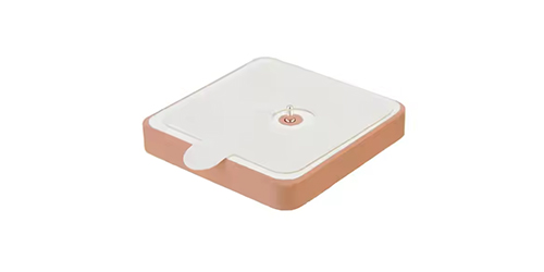
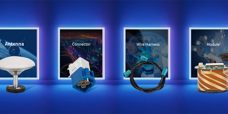
Products -PCBA Manufacturing RF Connectors RF Cable Assemblys Embedded Antennas External Antennas Positioning Chips and Modules
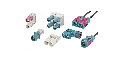
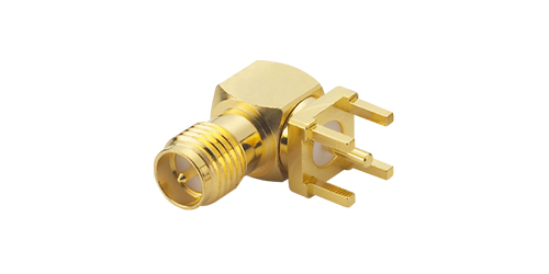
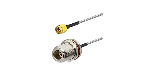
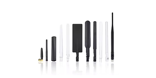
RF Connectors

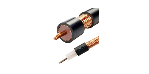
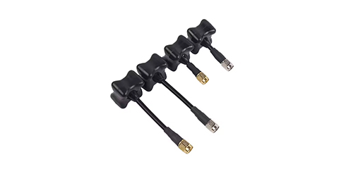
RF Cable Assemblys
Embedded Antennas
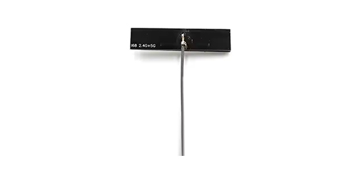
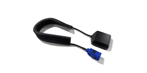
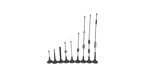
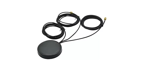
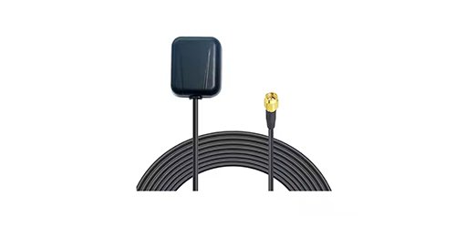
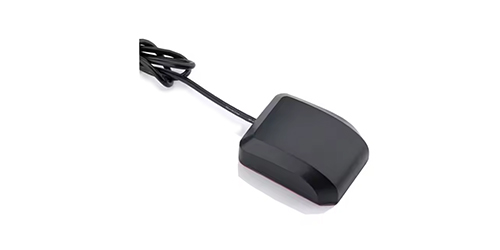
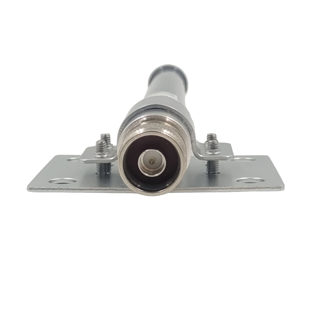
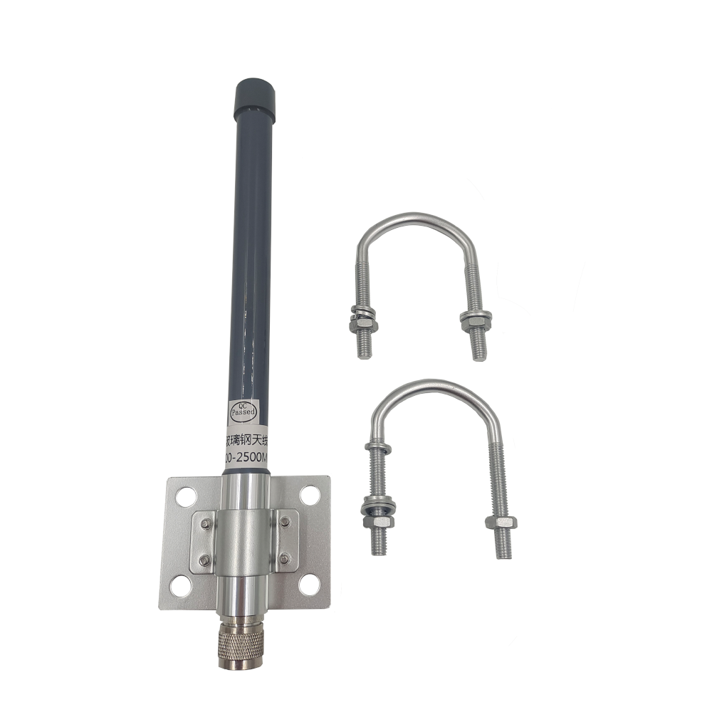
External Antennas
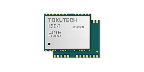
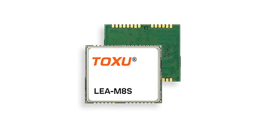
Positioning Chips and Modules


 Language


Language


The Global Positioning System (GPS) and other Global Navigation Satellite Systems (GNSS) like GLONASS, Galileo, and BeiDou have become the invisible utility underpinning modern life. From navigation and timing in smartphones to precision agriculture and autonomous vehicle guidance, the ability to pinpoint one's location on Earth is transformative. At the front end of every GNSS receiver is the antenna, the critical component responsible for capturing the incredibly weak signals broadcast from satellites orbiting over 20,000 kilometers away. Among the various antenna types, the Surface-Mount Device (SMD) GPS Antenna has emerged as the dominant form factor for the vast majority of modern consumer, industrial, and automotive applications.
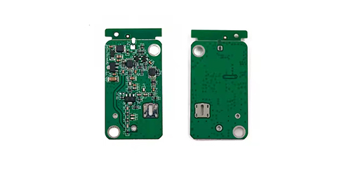
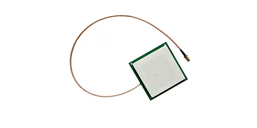
An SMD GPS Antenna is a complete, miniaturized antenna system designed to be mounted directly onto a printed circuit board (PCB) using standard automated surface-mount technology (SMT) soldering processes. Unlike external active antennas with coaxial connectors (e.g., helical or patch antennas in a radome), the SMD antenna is an integral part of the device's PCB assembly. This integration is the key to its ubiquity, enabling the proliferation of GPS functionality in increasingly compact and sleek devices like wearables, trackers, and smartphones.
The evolution towards SMD antennas is a story of the relentless drive for miniaturization, cost reduction, and manufacturing efficiency in electronics. Early GPS devices often featured external passive antennas, which were bulky and required careful placement for a clear view of the sky. The shift to active antennas (containing a Low-Noise Amplifier, or LNA) integrated into a plastic housing with a magnetic mount was a significant improvement for automotive and marine applications, but they remained separate components connected via a cable. The SMD antenna represents the next logical step: the complete elimination of the external component and its cable, integrating the antenna seamlessly into the device's own PCB layout.
This integration, however, comes with immense technical challenges. A GPS signal, by the time it reaches the Earth's surface, is vanishingly weak—often described as being "below the noise floor." The power received is typically around -130 dBm, which is considerably weaker than the thermal noise present in the receiver system. Therefore, the antenna must be exceptionally efficient at capturing this signal. Furthermore, it must be precisely tuned to the GPS L1 frequency (1575.42 MHz) and other GNSS bands, be resilient to environmental factors like temperature changes and physical proximity to other components, and maintain a consistent radiation pattern despite being placed inside a often-cluttered electronic device.
SMD GPS antennas are almost universally active antennas, meaning they incorporate a built-in Low-Noise Amplifier (LNA). This is non-negotiable for practical use. The signal loss from the antenna trace on the PCB to the GNSS receiver chip can be significant. Without amplification right at the source, this loss would devastate the system's noise figure, making the already-weak signals impossible to decipher from the noise. The LNA boosts the signal before any significant degradation occurs, preserving the crucial signal-to-noise ratio (SNR).
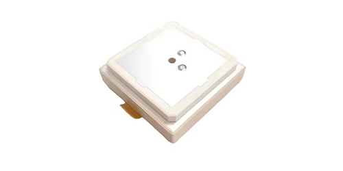
The physical form of an SMD GPS antenna is typically a small, rectangular ceramic block, often measuring between 10x10mm to 25x25mm with a height of just 2-4mm. The ceramic material is not just a housing; it is a critical part of the antenna's radiating structure, chosen for its specific dielectric properties that allow for effective miniaturization. The underside has metalized pads for soldering to the PCB, providing both mechanical attachment and electrical connection to the RF output and DC power for the LNA.
In summary, the SMD GPS antenna is a marvel of modern RF engineering and miniaturization. It is the enabling technology that allows virtually any electronic device to become location-aware without compromising on industrial design. Its overview is one of a highly specialized, integrated, and active component that performs the delicate task of listening to whispers from space, amplifying them, and delivering them to a receiver chip, all from a footprint smaller than a postage stamp.
The design and construction of an SMD GPS antenna is a sophisticated process that balances electromagnetic performance, mechanical robustness, manufacturability, and cost. It is a multi-disciplinary effort involving materials science, microwave engineering, and semiconductor design. Unlike a simple passive component, an SMD GPS antenna is a complex subsystem.
1. The Radiating Element: Ceramic and Geometry
The heart of the antenna is the radiating element, and its design is paramount.
Ceramic Core (Dielectric Resonator): The most common type of SMD GPS antenna is a ceramic patch antenna. A block of ceramic material with a high dielectric constant (εr typically between 20 and 40) is used. A high εr reduces the wavelength of the RF signal within the material (λ = λ₀ / √εr), allowing the physical size of the antenna to be shrunk while still resonating at the target 1.575 GHz frequency. Common materials include titanium-based ceramics, which offer a good balance of high εr, low loss tangent (for efficiency), and reasonable cost.
Patch and Feed Structure: The top surface of the ceramic block is metalized, often with silver, to form the actual radiating patch. The precise dimensions of this patch—its length and width—determine its resonant frequency. The antenna is fed by a specialized structure, often a probe feed or an aperture-coupled feed. In a probe feed, a pin connects from the feed point on the PCB through the ceramic to the patch. In aperture coupling, the patch is electromagnetically coupled to a microstrip feed line on the PCB through a slot in a ground plane. This method offers better bandwidth and isolation.
2. The Low-Noise Amplifier (LNA)
The integrated circuit is the "active" part of the active antenna.
Function: The LNA's primary role is to provide high gain (typically 15-30 dB) while adding as little internal noise as possible. Its performance is quantified by its Noise Figure (NF), which for a good GPS LNA is typically below 1 dB. A lower NF means better sensitivity.
Integration: The LNA is a bare die or a very small packaged IC placed directly on the antenna's substrate or on the small PCB that the ceramic radiator is mounted upon. It is positioned as close as physically possible to the feed point of the antenna to minimize any loss between the antenna and the amplifier input. This proximity is critical because even a fraction of a dB of loss before the LNA significantly degrades the overall system noise figure.
Biasing: The LNA requires DC power, which is supplied from the main device's board through the same RF output line via a bias tee circuit (or is fed on a separate line). The RF output from the antenna contains the amplified GPS signal riding on the DC voltage. The main GNSS receiver module on the device's PCB includes a capacitor to block this DC and extract the pure RF signal.
3. Layered Structure and Packaging
An SMD GPS antenna is a layered construction:
Base Substrate: A low-cost PCB substrate (like FR-4 or a more high-frequency laminate) forms the base. It contains the patterned traces for the RF output, DC supply, and ground.
Ceramic Radiator: The high-εr ceramic block is mounted and adhered to this base.
LNA Chip: The LNA die is bonded (e.g., with epoxy) and its pads are connected to the circuit traces via ultra-fine wire bonding.
Protective Casing: The entire assembly is typically encased in a protective plastic overmold. This mold serves several purposes: it protects the delicate wire bonds from physical damage and environmental factors (moisture, dust), and its material properties are carefully chosen to have minimal impact on the antenna's RF performance. It also provides the final SMD form factor with robust solderable pads.
4. The Critical Role of the Ground Plane
A fundamental aspect of patch antenna design, often overlooked, is the absolute necessity of a sufficient ground plane. The ceramic patch antenna does not operate in isolation; it functions as a resonant structure over a conductive surface. The device's PCB must provide a continuous, unbroken ground plane extending beyond the edges of the antenna itself. The size of this ground plane is a key factor in determining the antenna's performance characteristics, including its bandwidth, efficiency, and radiation pattern. Manufacturers provide detailed layout guidelines specifying the required keep-out area and minimum ground plane size. Placing the antenna too close to the edge of the PCB or over a void in the ground layer will severely degrade its performance.
5. Design and Simulation Process
The design is heavily reliant on advanced 3D electromagnetic (EM) simulation software like ANSYS HFSS or CST Studio Suite. Engineers model the exact geometry of the ceramic, the patch, the feed mechanism, the housing, and—critically—a model of the proposed PCB ground plane. The simulation optimizes parameters for:
Return Loss (S11): Ensuring good impedance matching (typically better than -10 dB) at 1575.42 MHz.
Radiation Pattern: Verifying a hemispherical pattern is achieved for maximum skyward gain.
Efficiency: Maximizing the ratio of radiated power to input power, a challenging task given the small size.
Bandwidth: Ensuring the antenna covers the necessary bandwidth for multi-GNSS support (e.g., ~1550-1610 MHz).
The construction is a precise endeavor, ensuring that the manufactured antennas have consistent performance with minimal unit-to-unit variation, a necessity for high-volume automated production.
The operation of an SMD GPS antenna is a two-stage process: first, the passive capture of electromagnetic waves, and second, the active amplification of the captured signal. Its principle of operation is rooted in fundamental antenna theory, but its effectiveness is entirely dependent on the meticulous integration of these two stages.
1. The Passive Radiating Principle: The Patch Antenna
The ceramic patch antenna operates as a resonant cavity. The metal patch on top and the device's ground plane on the bottom form the two walls of this cavity. The ceramic material between them is the dielectric filler. The antenna is designed so that its length L is approximately equal to half the wavelength of the GPS signal within the dielectric material (λ_g = c / (f * √εr)). At this resonant length, a standing wave of electric current is established on the patch.
The radiation mechanism is governed by the fringing fields at the edges of the patch. The electric field lines stretch from the patch, curve through the air, and terminate on the ground plane. These fringing fields are not entirely contained and are able to radiate energy into space. For reception, the process is reversed: the passing electromagnetic wave from a GPS satellite induces currents on the patch, which are then gathered at the feed point. The radiation pattern is typically directional broadside to the patch, meaning it is most sensitive to signals arriving from a direction perpendicular to the board's surface. This is ideal for GPS, as the satellites are generally above the horizon.
2. The Challenge of Weak Signals and the Need for an LNA
A GPS signal is spectacularly weak due to the immense distance it travels and the limited power of the satellite transmitters. By the time it reaches the Earth's surface, its power is around -125 to -130 dBm. To put this in perspective, this is billions of times weaker than the signal from a local cell tower. Furthermore, this signal is buried in thermal noise, which is present in all electronic systems.
The critical concept here is Noise Figure (NF). The noise figure of a system describes how much it degrades the signal-to-noise ratio (SNR). The first stage in any receiver chain has the most profound impact on the total system NF. This is articulated by Friis's formula.
If the passive antenna were connected directly via a trace on the PCB to the GNSS receiver chip, the loss in that trace (let's say 2-3 dB) would be the first "gain" stage (but it's a loss, so it's a negative gain). This loss would directly add to the system noise figure. A 3 dB loss means the system NF is at least 3 dB, drastically reducing sensitivity and making the GPS signals very difficult or impossible to acquire.
3. The Active Solution: Pre-Amplification
This is where the integrated LNA becomes non-negotiable. The LNA is placed infinitesimally close to the antenna's feed point. The weak RF current induced on the antenna by the satellite signal is delivered to the LNA input with virtually no loss.
The LNA then performs its crucial task: it amplifies the signal (both the desired GPS signal and the inherent noise present at its input) by a large factor (e.g., 100 to 1000 times, or 20-30 dB) while adding a minimal amount of its own internal noise (a low Noise Figure, e.g., 0.8 dB). The result is that the signal is boosted to a level that is strong enough to withstand the subsequent losses in the transmission line on the PCB to the GNSS receiver.
The output of the active antenna is therefore a much stronger version of the original signal. This amplified signal can then travel several centimeters across the main PCB with minimal relative degradation. The GNSS receiver chip then takes this signal and performs the complex tasks of down-conversion, correlation, and decoding to calculate the precise time and position.
4. The Role of Filtering
Many SMD GPS antennas also incorporate a bandpass filter either before or after the LNA. This filter is designed to allow frequencies in the GNSS band (approximately 1550-1610 MHz) to pass through while rejecting strong out-of-band signals from other services like cellular (700 MHz, 1.8 GHz, 2.1 GHz) and WiFi (2.4 GHz, 5 GHz). Without this filtering, these powerful interfering signals could overload the LNA, causing desensitization or distortion, which would again mask the weak GPS signals.
In essence, the working principle of the SMD GPS antenna is a battle against loss and noise. The passive ceramic patch efficiently captures the signal, and the integrated LNA immediately wins the first and most critical battle by boosting the signal above the noise floor before any significant loss can occur, enabling the entire positioning system to function.
The widespread adoption of SMD GPS antennas is driven by a compelling set of advantages that align perfectly with the needs of modern electronics manufacturing. However, this integrated approach also introduces specific challenges that engineers must carefully manage during product design.
Advantages:
Miniaturization and Form Factor: This is the primary advantage. SMD antennas are incredibly small and low-profile, allowing them to be integrated into devices where space is at a supreme premium, such as smartphones, wearables, fitness trackers, and asset tags. They enable sleek, compact product designs without the need for protruding external antennas.
Simplified Assembly and Reduced Cost:
Automated Manufacturing: As Surface-Mount Devices, they are perfectly suited for pick-and-place machines and reflow soldering processes. This allows for high-volume, automated assembly alongside all other PCB components, drastically reducing manufacturing time and labor costs compared to manually attaching and screwing in a external antenna with a connector.
Reduced Bill of Materials (BOM): They eliminate the need for a separate antenna component, a coaxial cable, and connectors (e.g., U.FL, SMA). This reduces part count, inventory complexity, and overall material cost.
Improved Reliability: Once soldered to the PCB, the SMD antenna becomes a solid, permanent part of the assembly. There are no cables to fray, no connectors to become loose through vibration or repeated mating/de-mating, and no external elements to be physically broken off. The overmolded package protects the internal components from moisture, dust, and mechanical shock.
Optimized Performance (when implemented correctly): The integration of the LNA directly at the antenna feed point provides the best possible system noise figure, as explained previously. This inherent advantage in sensitivity is a key performance benefit that is built into the design.
Design Consistency: Since the antenna is a pre-tested and pre-characterized module from the supplier, its performance is consistent and predictable. This reduces the RF design expertise required by the OEM and mitigates the risk of performance variations that can occur when designing a passive antenna from scratch on a PCB.
Challenges and Limitations:
PCB Layout Dependency: This is the single greatest challenge. The performance of an SMD patch antenna is highly dependent on the host PCB's design, specifically the size and shape of the ground plane. The antenna must be placed according to the manufacturer's strict guidelines, which always require a continuous ground plane extending a certain distance around the antenna. Placing it too close to the edge of the board, over a cut-out, or near large metal components (batteries, shields) will severely detune it and destroy its efficiency.
Sensitivity to Environment: The antenna's performance is affected by its immediate surroundings. The human body (especially the hand and head when in a phone) is a significant detuning element that can absorb RF energy and shift the antenna's resonant frequency. Similarly, placing the device on a metal car dashboard or against a wall can block or degrade signals. Designers must carefully consider the final product's enclosure and typical use-case scenarios.
Limited Bandwidth and Gain: Due to their small size, SMD antennas inherently have narrower bandwidth and lower gain compared to larger external antennas. While sufficient for standard GPS operations, this can be a limitation for advanced applications requiring multi-band, high-precision GNSS (e.g., L1/L2/L5 bands) or for use in environments with highly attenuated signals.
Thermal Considerations during Soldering: The ceramic body and internal components can be sensitive to the extreme thermal shock of reflow soldering. The product must be soldered using a profile that is compatible with the antenna's specifications to avoid cracking the ceramic or damaging the internal LNA.
Fixed Performance: Unlike an external antenna that can be repositioned for a better view of the sky, the performance of an SMD antenna is fixed by the device's orientation. This means the product industrial design must ensure the device is typically used in an orientation where the antenna has a clear view upward, not blocked by internal components or the user's hand.
In conclusion, the advantages of SMD GPS antennas—size, cost, and manufacturability—make them the default choice for mass-market applications. However, their successful implementation is not trivial. It requires careful RF layout and a thorough understanding of how the end product's design will influence the antenna's performance in the real world. The challenges are manageable but must be respected.
The SMD GPS antenna is a foundational component of the location-aware revolution. Its small size, low cost, and ease of integration have made GNSS technology ubiquitous across a staggering array of industries and consumer products. The applications are vast and growing, while future trends point towards even greater integration and performance.
Current Applications:
Consumer Electronics:
Smartphones and Tablets: The largest volume application. Provides location for navigation, geotagging, and location-based services.
Wearables: Fitness trackers and smartwatches (e.g., Garmin, Apple Watch) use them to track runs, cycles, and swims (in devices designed for it).
Cameras and Drones: Digital cameras use them for geotagging photos. Drones rely on them for precise positioning, hovering, and autonomous flight navigation.
Automotive and Telematics:
In-Vehicle Systems: Used for in-dash navigation systems, emergency eCall systems, and stolen vehicle tracking.
Telematics: Fleet management systems use SMD antennas in small dongles and trackers to monitor the location, speed, and routing of trucks and delivery vehicles. Usage-based insurance (UBI) devices also employ them.
Internet of Things (IoT) and M2M:
Asset Tracking: Small, battery-powered trackers attached to cargo containers, pallets, and high-value assets to provide global location data via cellular or satellite networks.
Smart Agriculture: GNSS guides tractors for precision planting and harvesting. Small sensors use it to tag data with location.
Industrial Monitoring: Sensors monitoring infrastructure (e.g., pipelines, electrical grids) often tag their readings with precise location and time stamps.
Personal and Pet Tracking: Small, lightweight tags that can be attached to a keychain, placed in a backpack, or on a pet's collar to allow owners to locate them via a smartphone app.
Future Trends:
Multi-Band and High-Precision GNSS:
The next generation of devices requires support for multiple frequencies (L1, L2, L5) from multiple constellations (GPS, Galileo, GLONASS, BeiDou). Using two frequencies allows the receiver to correct for ionospheric delay, enabling centimeter-level accuracy. Future SMD antennas will need to evolve from narrowband L1 patches to wider bandwidth designs that can cover from 1176 MHz (L5) to 1602 MHz (GLONASS L1) efficiently.
Tighter Integration: AiP (Antenna-in-Package) and AiM (Antenna-in-Module):
The trend is towards even greater integration. The next step is to move the antenna from being a discrete SMD component to being integrated into the same package as the GNSS receiver chip itself (AiP) or into a larger module that contains the receiver, memory, and other components (AiM). This saves further space and simplifies the PCB layout process even more, though it introduces new challenges in isolating the antenna from the noise of the digital IC.
Improved Resilience to Detuning:
Research is focused on making antennas more immune to their environment. Techniques include:
Reconfigurable Antennas: Using tunable components (like varactor diodes or RF switches) to dynamically adjust the antenna's resonant frequency if it is detuned by the presence of a hand or metal surface.
Field-Decoupling Techniques: Designing the antenna's structure to minimize currents induced on the device's ground plane, making its performance less dependent on ground plane size and nearby objects.
Hybrid Positioning Antennas:
As 5G evolves, a key trend is 5G positioning to complement GNSS, especially indoors and in urban canyons where satellite signals are weak. Future SMD antennas may be designed as multi-function components that can operate effectively across both GNSS and 5G positioning bands, all within a single footprint.
Enhanced Filtering for Coexistence:
Devices are becoming more crowded with radios (5G, WiFi 6E/7, Bluetooth, UWB). The RF environment is increasingly noisy. Future SMD GPS antennas will require even more robust and selective filtering integrated directly alongside the LNA to reject this powerful interference and prevent jamming of the sensitive GNSS receiver.
The SMD GPS antenna will continue to be a critical enabling technology. Its future is not one of replacement but of evolution—becoming more integrated, more intelligent, more broadband, and more resilient, continuing to provide the vital link to satellite constellations for an ever-expanding universe of connected devices.
Conclusion
The SMD GPS antenna is a quintessential example of how technological evolution driven by the demands of miniaturization and mass production can yield a component that is both highly sophisticated and deceptively simple in its final application. It represents the culmination of advancements in ceramic materials, microwave engineering, semiconductor design, and automated manufacturing, all converging to solve a critical problem: how to hear whispers from space from within the confines of a pocket-sized electronic device.
From its overview as a complete integrated subsystem to the intricacies of its design centered on a high-dielectric ceramic resonator, the SMD antenna is a masterpiece of RF engineering. Its working principle hinges on the critical act of immediate signal amplification at the feed point, a strategy that preserves the precious signal-to-noise ratio of the incredibly weak GNSS signals. This core function is what enables everything that follows in the receiver chain.
The advantages it offers—unmatched compactness, manufacturing efficiency, cost-effectiveness, and reliability—are so compelling that it has become the undisputed standard for integrating GNSS functionality into virtually every consumer and industrial product imaginable. It has democratized access to precise positioning and timing, enabling innovations from fitness tracking to autonomous systems.
However, as detailed, its integration is not without challenges. Its performance is inextricably linked to the design of the product it is placed within. The absolute necessity of a proper ground plane and a thoughtful layout cannot be overstated; failure to adhere to these RF principles results in a non-functional GPS feature, a costly mistake in any product development cycle. Furthermore, its inherent limitations in bandwidth and gain, alongside its sensitivity to the operating environment, define the boundaries within which it operates best.
Looking forward, the SMD GPS antenna is not a static technology. The trends are clear: it will evolve to support the demands for higher precision through multi-band operation, become even more integrated through AiP and AiM technologies, and grow smarter with features like reconfigurability to combat real-world detuning. It will remain at the forefront, enabling new applications in the IoT, automotive, and consumer spaces.
In conclusion, the SMD GPS antenna is far more than a simple component. It is a vital bridge between the physical world and the digital realm of location data. Its successful implementation is a key differentiator in product design, balancing the competing demands of performance, size, cost, and time-to-market. As our world becomes ever more connected and location-aware, this small, unassuming ceramic block will continue to play an indispensable role in guiding the way.

 86 0755 2819 9597
Lucy Yang | lucy.y@toxutech.com
Nicole Li | nicole@toxutech.com
Dotty Zhao | sales04@toxutech.com
Global Business Director / Sales Team / Global Operations


 En
En Cn
Cn Korean
 Home >


