

-
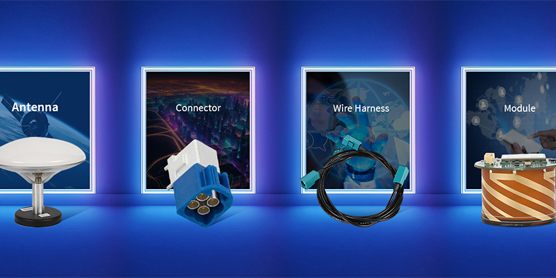
Products -PCBA Manufacturing RF Connectors RF Cable Assemblys Embedded Antennas External Antennas Positioning Chips and Modules
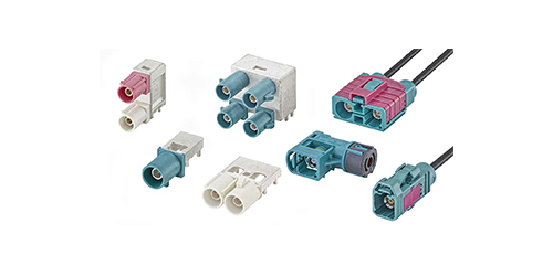
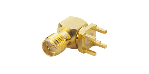
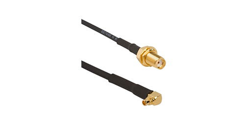
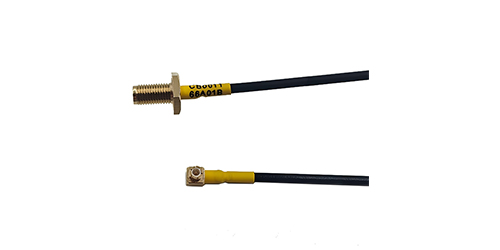
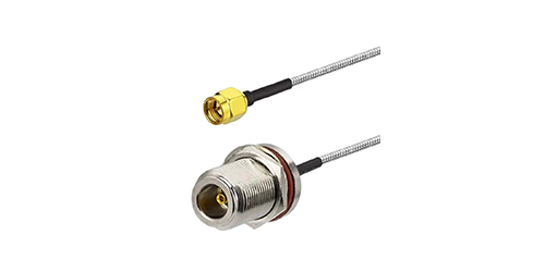
RF Connectors

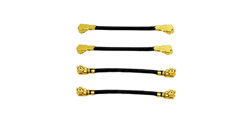
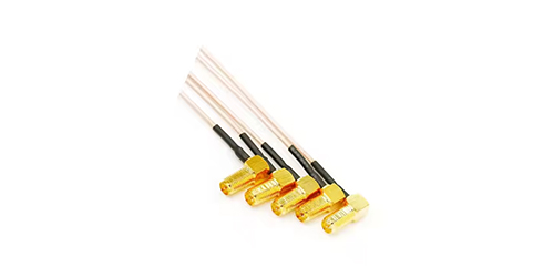
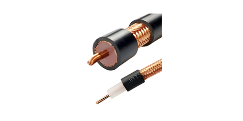
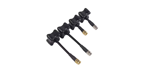
RF Cable Assemblys
Embedded Antennas
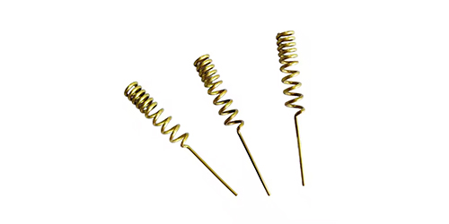
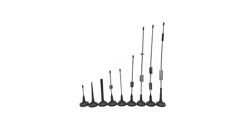
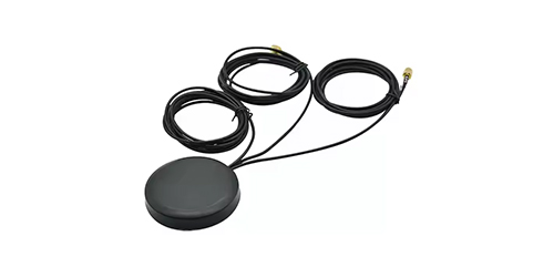
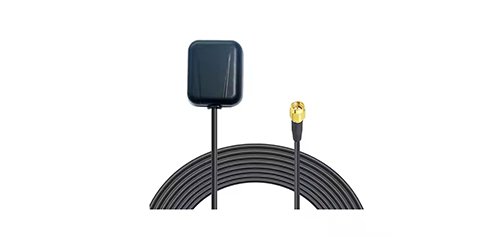
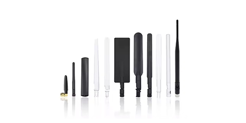
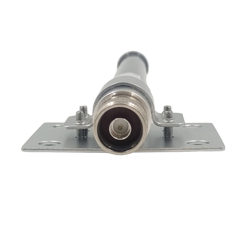
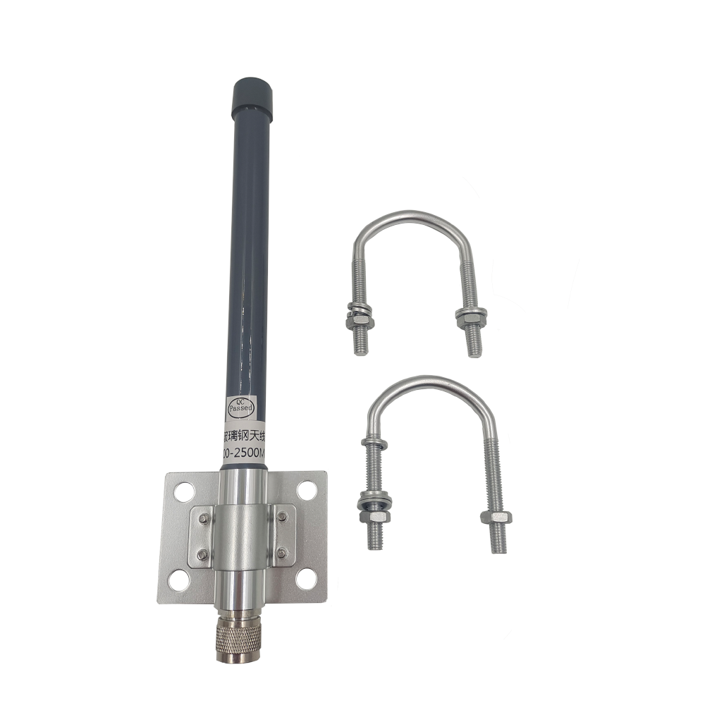
External Antennas
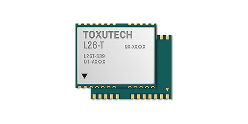
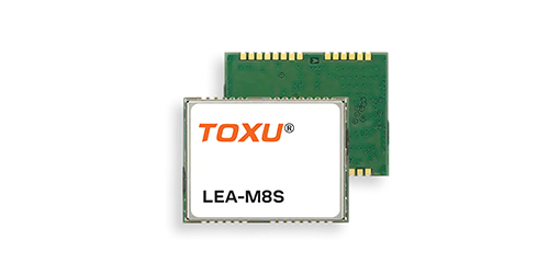
Positioning Chips and Modules


 Language


Language


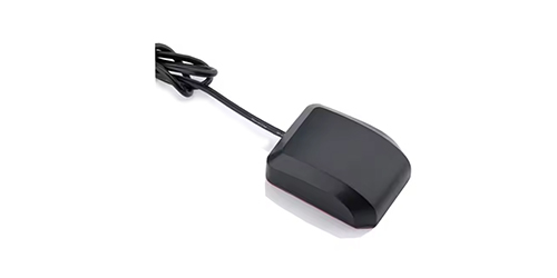
In the rapidly expanding landscape of the Internet of Things (IoT), where billions of devices are interconnected to collect, exchange, and analyze data, precise location information has become a fundamental requirement for numerous applications. Mini Surface Mount Device (SMD) GPS antennas have emerged as a critical enabling technology, catering to the unique needs of IoT devices. These antennas combine compact size, efficient performance, and ease of integration, making them ideal for a wide range of IoT applications that demand accurate positioning capabilities.
The IoT ecosystem encompasses a vast array of devices, from smart home appliances and wearable fitness trackers to industrial sensors and autonomous vehicles. Many of these devices rely on Global Positioning System (GPS) technology to determine their location, which is essential for functions such as asset tracking, navigation, logistics management, and environmental monitoring. However, IoT devices often have limited space, strict power consumption requirements, and need to operate in diverse and sometimes challenging environments. Traditional GPS antennas may not be suitable due to their size, power usage, or inability to integrate seamlessly with the small - form - factor design of IoT devices.
Mini SMD GPS antennas address these challenges. The “SMD” refers to the manufacturing and mounting technique, where the antenna is designed to be directly soldered onto a printed circuit board (PCB) of the IoT device. This surface - mount technology enables a more compact and streamlined design, reducing the overall footprint of the antenna within the device. The “mini” aspect emphasizes the small physical size of the antenna, which is crucial for fitting into the increasingly miniaturized IoT devices. Despite their small size, these antennas are engineered to efficiently receive the weak GPS signals transmitted by satellites, which typically have a power level of around -160 dBm when reaching the Earth's surface.
These antennas play a pivotal role in enhancing the functionality and capabilities of IoT devices. For example, in a supply chain management scenario, mini SMD GPS antennas integrated into shipping containers can provide real - time location data, enabling companies to track the movement of goods, optimize routes, and improve delivery efficiency. In smart cities, IoT - enabled streetlights equipped with these antennas can be precisely located for maintenance and management purposes. As the IoT market continues to grow exponentially, the demand for mini SMD GPS antennas is expected to surge, driving further innovation and development in this field.
The design and construction of a mini SMD GPS antenna for IoT devices involve a meticulous combination of antenna engineering, microfabrication techniques, and a deep understanding of the specific requirements of IoT applications. The antenna is typically composed of several key components, each carefully designed to ensure optimal performance, compactness, and ease of integration.
Antenna Element Design
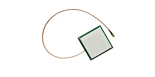
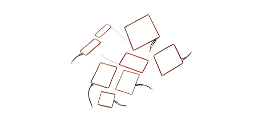
The antenna element is the core component responsible for capturing the weak GPS signals from satellites. In mini SMD GPS antennas, planar antenna designs are commonly used due to their suitability for surface - mount technology and ability to be integrated into small spaces. One of the most prevalent types is the microstrip antenna, which consists of a metallic patch (usually made of copper or gold) on a dielectric substrate, with a ground plane beneath it.
The design of the metallic patch is crucial for determining the antenna's resonant frequency and radiation pattern. The shape, size, and configuration of the patch are optimized through electromagnetic simulations to resonate at the specific frequencies of GPS signals, mainly in the L - band range (e.g., 1.575 GHz for the L1 band). Advanced simulation software allows engineers to fine - tune the patch design to achieve high gain, good impedance matching, and a suitable radiation pattern that can effectively receive signals from different satellite directions.
The dielectric substrate also plays a vital role. It is selected for its electrical properties, such as dielectric constant and loss tangent. A substrate with a high dielectric constant can help in reducing the physical size of the antenna, while a low loss tangent minimizes signal losses. Common dielectric materials used include FR4 (a type of fiberglass - epoxy laminate), Rogers RT/duroid series, and ceramic - based substrates. The choice of substrate depends on factors such as the desired antenna size, performance requirements, and cost considerations.
Integration with IoT Device PCBs
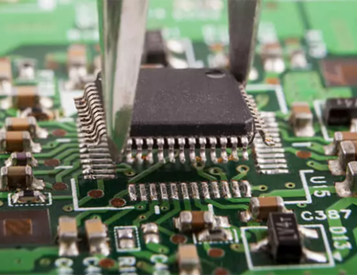
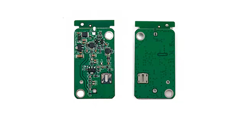
The integration of the mini SMD GPS antenna with the IoT device's PCB is a critical aspect of its design. The antenna is designed to be directly soldered onto the PCB using surface - mount technology. This requires precise alignment of the antenna pads with the corresponding pads on the PCB. To facilitate this, the antenna is often provided with a standard SMD package, which has specific pad dimensions and pitch that are compatible with industry - standard PCB assembly processes.
During the design phase, the layout of the PCB around the antenna area is carefully planned to minimize electromagnetic interference (EMI) and ensure proper signal integrity. The ground plane of the PCB is designed to act as a reflector for the antenna, enhancing its radiation efficiency. Specialized techniques such as ground plane shaping, slotting, and the use of vias are employed to optimize the interaction between the antenna and the PCB ground plane.
In addition, the connection between the antenna and the subsequent signal processing components on the PCB, such as the low - noise amplifier (LNA) and the GPS receiver, is carefully designed. The routing of the signal traces from the antenna to these components is done with consideration for impedance matching, signal attenuation, and EMI suppression. Proper shielding and isolation techniques may also be used to protect the sensitive GPS signals from interference generated by other components on the PCB.
Materials and Packaging
The choice of materials for a mini SMD GPS antenna is crucial for its performance, durability, and compatibility with IoT devices. The metallic patch of the antenna is typically made of highly conductive materials like copper or gold. Copper is commonly used due to its good conductivity and relatively low cost, while gold may be preferred in some high - performance or harsh - environment applications for its excellent corrosion resistance.
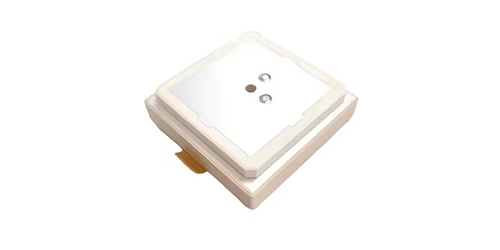
The packaging of the mini SMD GPS antenna is designed to protect the internal components and provide a robust structure for surface - mount assembly. The antenna is often encapsulated in a plastic or ceramic housing. Plastic packages are cost - effective and offer good mechanical protection, while ceramic packages can provide better electrical performance and thermal stability, making them suitable for high - performance or high - temperature applications.
The packaging also includes features for easy handling and soldering during the PCB assembly process. It may have clearly defined pads, alignment marks, and a flat surface to ensure proper soldering and mechanical stability on the PCB. The dimensions and shape of the package are optimized to minimize the space occupied by the antenna on the PCB, while still providing sufficient protection for the internal antenna element and any associated components.
The working principles of a mini SMD GPS antenna for IoT devices are based on the fundamental concepts of satellite communication and signal processing, adapted to the compact and resource - constrained nature of IoT applications. The antenna operates in conjunction with a GPS receiver to enable accurate positioning of the IoT device.
Signal Reception
The process begins with the antenna element capturing the weak radio - frequency signals transmitted by GPS satellites. These signals, which carry information about the satellite's position and time, travel through the Earth's atmosphere and reach the antenna. The mini SMD GPS antenna, with its carefully designed resonant frequency and radiation pattern, is engineered to efficiently couple with the incoming GPS signals.
When the frequency of the incoming GPS signals matches the resonant frequency of the antenna, a resonance effect occurs. This resonance enhances the antenna's ability to absorb the energy of the signals, converting the electromagnetic energy of the GPS signals into electrical signals. The metallic patch on the antenna plays a key role in this process, as it interacts with the electromagnetic fields of the GPS signals, generating induced electrical currents that represent the received signals. However, these initial electrical signals are extremely weak and require further processing to be useful for the GPS receiver.
Signal Amplification and Filtering
The weak electrical signals generated by the antenna element are then fed into a low - noise amplifier (LNA), which is often integrated with the antenna or located nearby on the PCB. The primary function of the LNA is to amplify the weak GPS signals while adding minimal noise to them. This is crucial because the signals received from the satellites are already very weak, and any additional noise could degrade the accuracy of the positioning calculations.
After amplification, the signals pass through a series of filters. Band - pass filters are commonly used to allow only the frequencies within the GPS signal band to pass through while attenuating frequencies outside this band. This helps to reject interference from other radio - frequency sources operating at different frequencies, such as wireless communication devices or electrical equipment. Additionally, notch filters may be employed to specifically target and attenuate certain frequencies that are known to cause interference, further improving the signal quality.
Signal Transmission to the GPS Receiver
The filtered and amplified signals are then transmitted to the GPS receiver on the IoT device. The GPS receiver uses these signals to calculate the time - of - arrival (TOA) or time - difference - of - arrival (TDOA) of the signals from multiple satellites. By knowing the speed of light and the time it takes for the signals to travel from the satellites to the antenna, the receiver can calculate the range between the IoT device and each satellite. Using the principle of trilateration, the receiver combines the range measurements from at least four satellites to determine the precise location of the IoT device in three - dimensional space (latitude, longitude, and altitude).
The mini SMD GPS antenna's role in this process is to ensure that the GPS receiver receives strong and clean signals. Its efficient signal reception, amplification, and filtering capabilities are essential for accurate positioning, even in challenging environments where the GPS signals may be weak or subject to interference.
Advantages
One of the most significant advantages of mini SMD GPS antennas for IoT devices is their compact size. Their small physical dimensions make them highly suitable for integration into the limited space available in IoT devices, which are often designed to be small and lightweight. This compactness enables the development of sleek and portable IoT products, such as wearable devices and small - form - factor sensors, without sacrificing the essential GPS positioning functionality.
Another key advantage is their ease of integration. The surface - mount design allows for straightforward assembly onto the IoT device's PCB using standard manufacturing processes. This reduces the complexity of the device design and manufacturing, enabling faster production cycles and lower manufacturing costs. The compatibility with industry - standard PCB assembly techniques also makes it easier for manufacturers to scale up production and integrate the antennas into a wide range of IoT products.
Mini SMD GPS antennas also offer good performance despite their small size. Advanced design and simulation techniques enable engineers to optimize the antenna's radiation pattern, gain, and impedance matching, ensuring efficient signal reception. The integration of low - noise amplifiers and filters with the antenna helps in enhancing the signal quality and reducing the impact of interference, resulting in accurate positioning even in challenging environments.
In addition, these antennas are relatively cost - effective. The use of mass - producible materials and standard manufacturing processes helps in keeping the production costs low. This affordability makes them accessible for a wide range of IoT applications, from consumer - oriented devices to large - scale industrial IoT deployments, where cost - effectiveness is a crucial factor.
Challenges
Despite their numerous advantages, mini SMD GPS antennas for IoT devices face several challenges. One of the primary challenges is electromagnetic interference (EMI). IoT devices often contain multiple electronic components, such as wireless communication modules, microcontrollers, and power management circuits, which can generate electromagnetic fields that interfere with the operation of the GPS antenna. To mitigate EMI, careful PCB layout design, shielding techniques, and the use of EMI - suppressing components are required. However, implementing these measures can increase the complexity and cost of the IoT device design.
Another challenge is related to the power consumption of the antenna and its associated components, such as the LNA. In battery - powered IoT devices, minimizing power consumption is crucial for extending the device's operating life. While efforts are made to design low - power LNAs and efficient antenna circuits, the power consumption can still be a limiting factor, especially for devices that require continuous GPS tracking. Developing more energy - efficient antenna designs and components is an ongoing area of research.
Environmental factors also pose a challenge. IoT devices are often deployed in diverse environments, ranging from harsh industrial settings to outdoor and mobile applications. Mini SMD GPS antennas need to be able to withstand extreme temperatures, humidity, vibration, and physical impacts. Ensuring the durability and reliability of the antennas in these environments requires the use of robust materials and packaging, which may add to the cost and size of the antenna.
Finally, achieving high - accuracy positioning in all types of environments is a challenge. In urban areas, for example, buildings can block or reflect GPS signals, causing multipath interference, which can degrade the accuracy of the positioning. Similarly, in areas with limited satellite visibility, such as dense forests or indoor environments, obtaining accurate location information can be difficult. Developing techniques to improve the antenna's performance in these challenging environments is an important area of focus for researchers and manufacturers.
Applications
Mini SMD GPS antennas have a wide range of applications in the IoT domain. In the consumer electronics sector, they are commonly used in wearable devices such as smartwatches, fitness trackers, and child - tracking devices. These devices rely on GPS positioning to provide users with accurate location information for activities like fitness tracking, navigation, and safety monitoring.
In the logistics and supply chain management industry, mini SMD GPS antennas are integrated into shipping containers, pallets, and vehicles. This enables real - time tracking of goods, allowing companies to optimize routes, monitor delivery schedules, and improve the overall efficiency of their supply chain operations. It also helps in reducing losses due to theft or misplacement of goods.
For industrial IoT applications, these antennas are used in asset tracking systems for monitoring the location of valuable equipment, machinery, and tools within factories and industrial sites. They are also employed in environmental monitoring devices, such as weather sensors and pollution monitors, which need to be precisely located to provide accurate data.
In the automotive IoT segment, mini SMD GPS antennas are used in connected cars for navigation, vehicle tracking, and emergency response systems. They are also integrated into autonomous vehicles to provide accurate positioning information, which is essential for safe and efficient operation.
Future Trends
Looking ahead, several future trends are expected to shape the development of mini SMD GPS antennas for IoT devices. One significant trend is the integration of multiple satellite navigation systems. In addition to GPS, other global navigation satellite systems (GNSS) such as GLONASS, Galileo, and BeiDou are becoming more prevalent. Future antennas will be designed to receive signals from multiple GNSS simultaneously, providing greater redundancy and enhanced accuracy, especially in areas where GPS signals alone may not be sufficient.
The miniaturization of these antennas will continue, driven by the increasing demand for smaller and more compact IoT devices. New materials and manufacturing techniques, such as nanotechnology and 3D printing, will be explored to further reduce the size of the antennas without sacrificing performance. This will enable the integration of GPS functionality into even smaller and more specialized IoT devices, such as implantable medical sensors and tiny environmental monitors.
The integration of artificial intelligence (AI) and machine learning (ML) with mini SMD GPS antennas is an emerging trend. AI and ML algorithms can be used to optimize the performance of the antenna, adapt to changing environmental conditions, and improve signal processing in the presence of interference. For example, AI can analyze real - time data from the antenna and other sensors to predict and mitigate the effects of multipath interference, enhancing the overall accuracy and reliability of the positioning system.
There is also a growing interest in using these antennas for indoor positioning. While traditional GPS is mainly effective outdoors, researchers are exploring ways to adapt the technology for indoor environments, such as shopping malls, airports, and office buildings. Mini SMD GPS antennas, with their advanced signal processing capabilities and compact size, may play a crucial role in developing accurate indoor positioning systems for IoT applications.
Conclusion
In conclusion, mini SMD GPS antennas have become an essential component for IoT devices, enabling accurate positioning in a wide range of applications. Their compact size, ease of integration, good performance, and cost - effectiveness make them well - suited for the diverse and rapidly evolving IoT ecosystem.
However, challenges such as electromagnetic interference, power consumption, environmental factors, and achieving high - accuracy positioning in all environments need to be addressed. Overcoming these challenges will require continuous innovation in design, materials, and manufacturing processes, as well as the development of new technologies and algorithms.
As the IoT market continues to expand, the future of mini SMD GPS antennas looks promising. With trends such as multi - GNSS integration, further miniaturization, the integration of AI and ML, and indoor positioning on the horizon, these antennas will continue to evolve and play an even more significant role in enhancing the functionality and capabilities of IoT devices. They will contribute to the creation of a more connected, intelligent, and efficient world, where accurate location information is seamlessly integrated into the fabric of our daily lives and industrial operations.

 86 0755 2819 9597
Lucy Yang | lucy.y@toxutech.com
Nicole Li | nicole@toxutech.com
Dotty Zhao | sales04@toxutech.com
Global Business Director / Sales Team / Global Operations


 En
En Cn
Cn Korean
 Home >


