

-
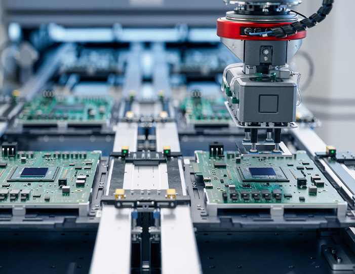
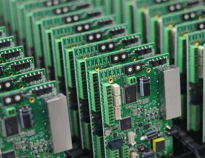
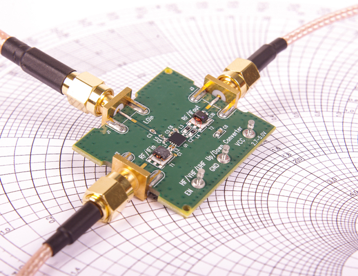
Products -PCBA Manufacturing RF Connectors RF Cable Assemblys Embedded Antennas External Antennas Positioning Chips and Modules
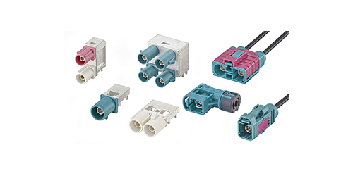
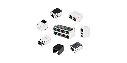
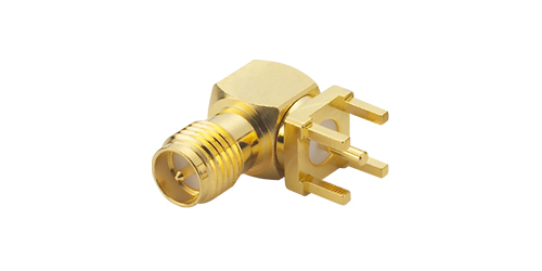
RF Connectors

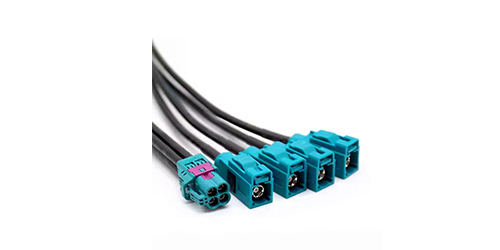
RF Cable Assemblys
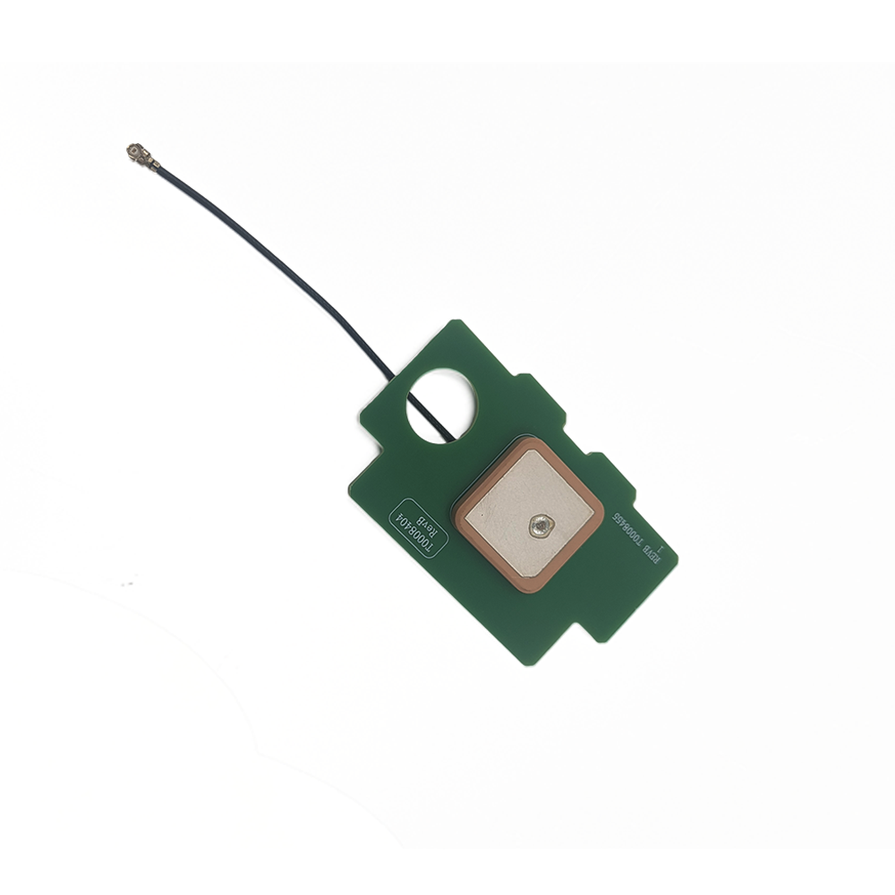
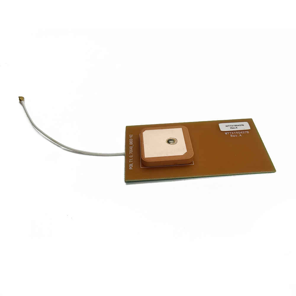
Embedded Antennas
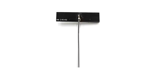
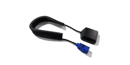
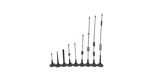
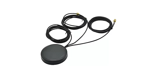
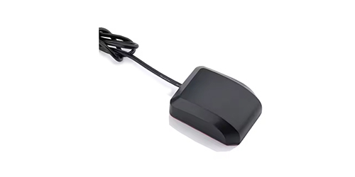
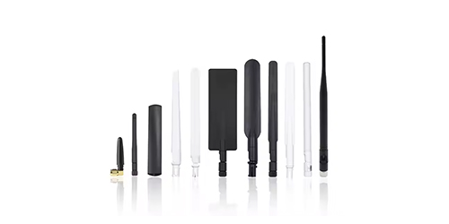
External Antennas
Positioning Chips and Modules
 Language


Language

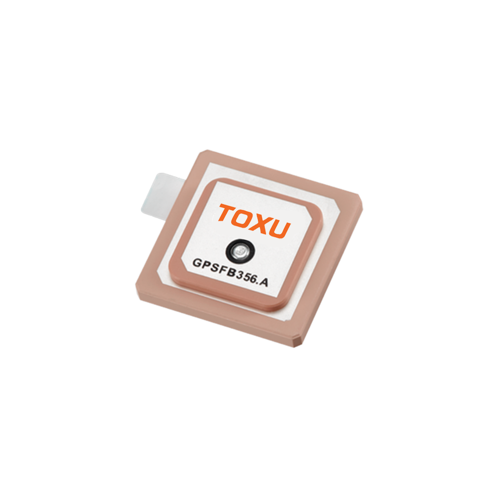
In the modern world, the ability to know one's location is often taken for granted. This capability is enabled by the Global Positioning System (GPS) and other Global Navigation Satellite Systems (GNSS), a complex constellation of technologies. While the satellites in space and the processors in our devices capture the imagination, a critical and often overlooked component resides within the device itself: the integrated GPS ceramic patch antenna. This unassuming, flat square is the fundamental gateway that connects our personal electronics, vehicles, and countless other devices to the vast infrastructure of satellite navigation. It represents the triumph of miniaturization, cost-effectiveness, and mass production, bringing the power of GPS from the specialized realm of surveyors into the pockets of billions.
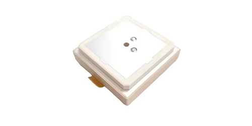
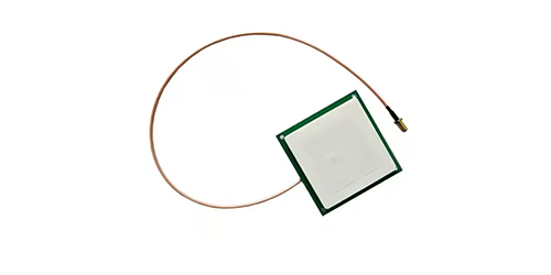
An integrated ceramic patch antenna is a type of microstrip antenna designed to be mounted directly onto a printed circuit board (PCB) inside an electronic device. Unlike external active antennas with their separate cables and connectors, this antenna is a "patch" of conductive material fused onto a ceramic substrate, becoming a permanent and seamless part of the product's internal architecture. Its primary function is to receive the incredibly weak L1 frequency (1575.42 MHz) signals broadcast from GPS satellites orbiting over 20,000 kilometers away. The "integrated" aspect is key; it is not an accessory but a built-in feature, enabling the sleek, compact form factors we expect in smartphones, wearables, drones, and asset trackers.
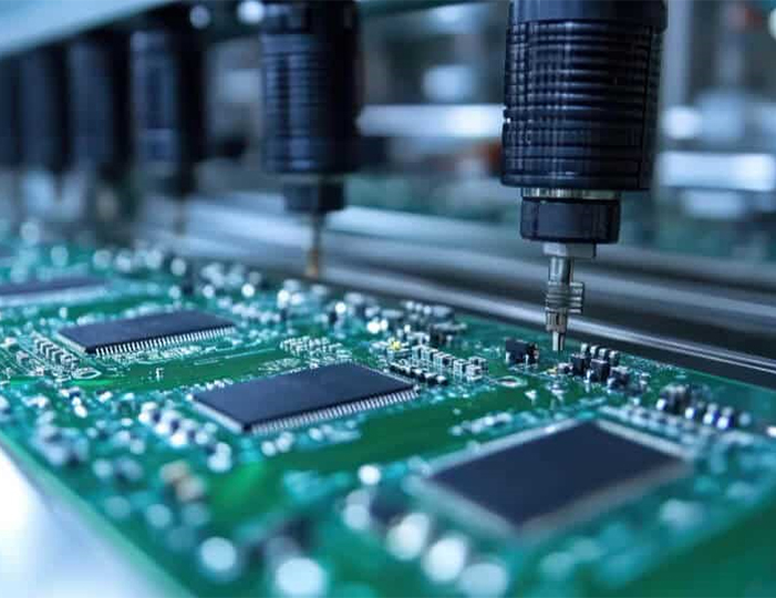
The driving force behind the development and dominance of this antenna type is the consumer electronics revolution. The demand for smaller, lighter, and cheaper devices necessitated a GPS solution that was equally miniaturized, required no external parts, and could be automated in high-volume assembly. The ceramic patch antenna met all these criteria. It offered a low-profile design that could be surface-mounted (SMD) by a pick-and-place machine alongside resistors and capacitors, drastically reducing assembly time and cost compared to installing a separate antenna module.
However, this integration comes with a unique set of challenges. Placing an antenna inside a device is an electromagnetic compromise. The device's own metal components, battery, display, and the user's hand can all detune the antenna, block signals, and create multipath interference. Therefore, the design of a ceramic patch antenna is not just about the antenna itself, but about its intricate relationship with the device it inhabits. Its performance is a result of a careful dance between the antenna designer, the RF engineer, and the product designer, who must allocate precious real estate within the device for this critical component.
These antennas are the workhorses of consumer-grade positioning. They are not typically designed for the centimeter-level accuracy required by surveyors, which demands dual-frequency reception and ultra-stable phase characteristics. Instead, their goal is to provide reliable, meter-level accuracy for navigation, location-based services, fitness tracking, and logistics. They enable the "blue dot" on our phone maps, the geotagging of our photos, the tracking of a delivery truck, and the autonomous return-to-home function of a drone. The integrated ceramic patch antenna is the unsung hero of the location economy, a masterpiece of miniaturization that has made GPS a ubiquitous and invisible utility in our daily lives.
The design and construction of an integrated GPS ceramic patch antenna is a sophisticated exercise in microwave engineering and materials science, focused on achieving reliable performance within the severe constraints of a consumer electronic device's interior. Every aspect of its form and composition is a carefully considered compromise between size, cost, efficiency, and bandwidth.
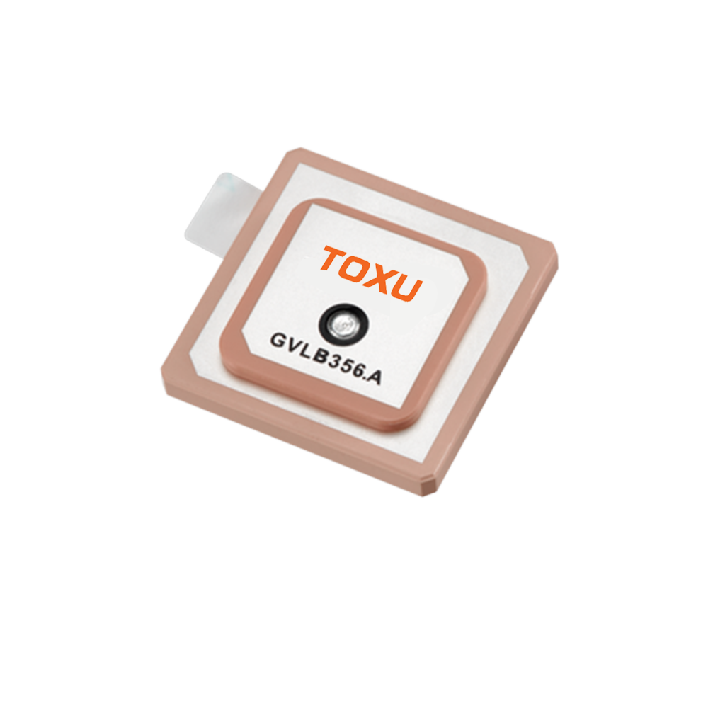
The foundation of the antenna is the ceramic substrate. This is not ordinary pottery clay but a precisely engineered material, typically a blend of titanium dioxide or barium tetratitanate. The key property of this ceramic is its very high dielectric constant (εr), often ranging from 20 to 40 and sometimes higher. A high dielectric constant is crucial for miniaturization because the wavelength of an electromagnetic wave inside a material is inversely proportional to the square root of εr. A higher εr effectively "slows down" the wave, allowing the antenna to be physically smaller while still resonating at the target GPS frequency of 1.575 GHz. The substrate is fired into a rigid, monolithic block, providing a stable and consistent platform for the radiating element.
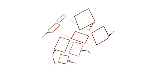
On top of this ceramic block, the radiating patch is fabricated. This is a square or rectangular layer of conductive material, usually silver or a silver-palladium alloy, applied through a screen-printing and sintering process. The size of this patch is the primary determinant of the resonant frequency. Using the high-dielectric ceramic allows this patch to be remarkably small, often between 10mm x 10mm and 25mm x 25mm, with a thickness of just 3mm to 4mm. The precise dimensions and shape are fine-tuned using electromagnetic simulation software to optimize performance metrics like impedance bandwidth and radiation efficiency.
The underside of the ceramic block is a continuous layer of metal, forming the ground plane. This is a non-negotiable requirement for a patch antenna. The ground plane acts as an electrical reflector, directing the antenna's radiation pattern away from the device's internals and towards the outside world. It creates the necessary capacitance with the radiating patch to establish resonance. The size of the ground plane on the host PCB is critically important; a ground plane that is too small will severely degrade antenna performance, detune its frequency, and distort its radiation pattern. Antenna manufacturers provide strict layout guidelines specifying the minimum required ground plane size and the keep-out areas free of other components.
The antenna is connected to the device's GPS receiver via a 50-ohm feed line on the PCB. The feed point—where the RF energy is transferred from the antenna to the circuit—is a critical design parameter. It can be fed using a microstrip line directly connected to the edge of the patch, or more commonly, through a probe feed where a pin from the underside of the ceramic (connected to the PCB trace) extends up and makes contact with the patch. This method allows for impedance matching by precisely positioning the feed point.
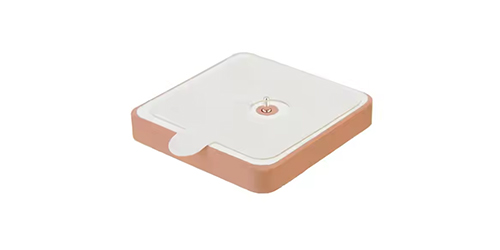
Integration is the final and most complex step. The antenna is typically supplied as a Surface-Mount Device (SMD) with metallized terminals on its base. It is soldered onto the PCB during reflow soldering, just like any other component. However, its location is paramount. It must be positioned at the periphery of the device, ideally near a plastic or glass window in the casing that is RF-transparent. Designers often place it at the top of a smartphone or in the arms of a drone, away from the major sources of interference: the lithium-ion battery (a large RF-absorbing mass), the display (a source of noise), and the user's hand (a bag of lossy saltwater that can block signals and detune the antenna).
To mitigate these integration challenges, many modern ceramic patches incorporate a built-in Low-Noise Amplifier (LNA). This is a tiny semiconductor chip embedded within the antenna assembly or mounted on a small PCB directly attached to it. This "active" antenna configuration amplifies the weak satellite signals right at the source, before they are attenuated by the transmission line and corrupted by the noise figure of the main receiver. This significantly improves sensitivity and helps overcome the performance losses inherent in being housed inside a compromised environment.
The operational principle of an integrated ceramic patch antenna is a story of resilience, a constant battle to capture faint signals from space while operating inside the electromagnetically hostile confines of its host device. Its function is more nuanced than that of an external antenna; it must work with its environment, as it cannot escape it.
The process begins when the right-hand circularly polarized (RHCP) electromagnetic wave from a GPS satellite penetrates the device's outer casing. The wave induces an oscillating electric field between the radiating patch and the ground plane. The high-dielectric ceramic substrate concentrates this field, allowing the small patch to efficiently resonate at the 1.575 GHz frequency. This resonance converts the energy of the passing wave into a tiny oscillating voltage at the feed point.
This initial signal is astonishingly weak, typically around -130 dBm (decibels relative to one milliwatt). It is at this most vulnerable stage that the integrated LNA, if present, performs its critical role. By providing 15-25 dB of gain with an ultra-low noise figure (often < 1.5 dB), it boosts the signal strength well above the thermal noise floor. This is crucial because the signal must then travel along a microstrip trace on the PCB to the GPS receiver chip. This trace, no matter how well designed, introduces some loss. The pre-amplification ensures that the signal arriving at the receiver is strong and clean enough for processing.
The antenna's radiation pattern is fundamentally shaped by its design and placement. In free space, a patch antenna has a hemispherical pattern, radiating broadly upwards. However, when integrated into a device, this pattern is dramatically distorted. The metal ground plane blocks radiation downwards into the device. The device's chassis, battery, and other components act as parasitic elements, reflecting, absorbing, and scattering the energy. The resulting pattern is often a complex, irregular lobe directed outwards from the device's "window." This is why device orientation matters; tilting the device can move the antenna's "view" of the sky, potentially blocking satellites and degrading accuracy.
A constant challenge is detuning. The antenna is designed to have a specific impedance (50 ohms) at its resonant frequency. However, the proximity of other materials—especially the user's hand or head—alters the electromagnetic fields around the antenna. This shifts its resonant frequency and changes its impedance, causing a impedance mismatch. When mismatched, a portion of the precious signal power is reflected back from the antenna instead of being delivered to the receiver, drastically reducing efficiency. Modern devices often employ sophisticated adaptive impedance matching networks—small circuits that can dynamically adjust to compensate for these detuning effects in real-time, ensuring maximum power transfer regardless of how the device is held.
Finally, the amplified signal is delivered to the GPS receiver IC (Integrated Circuit). This chip performs the heavy lifting: it down-converts the RF signal, correlates it with replica C/A codes to acquire the satellites, and performs the calculations to derive a position, velocity, and time (PVT) solution. The quality of the raw signal provided by the ceramic patch antenna and its LNA directly determines how quickly the receiver can achieve a Time to First Fix (TTFF) and how well it can maintain satellite lock in challenging signal environments, such as under tree cover or in urban canyons. The antenna doesn't process information, but it defines the quality of the raw material that the processor uses to build a location.
The integrated ceramic patch antenna offers a compelling set of advantages that have cemented its dominance in consumer electronics, but these benefits are inextricably linked to a set of significant engineering challenges.
Advantages:
Extreme Miniaturization and Low Profile: This is the primary advantage. The high-dielectric ceramic allows for a remarkably small form factor that can be embedded into the slimmest of devices, enabling the sleek industrial designs demanded by the market.
Low Cost and High-Volume Manufacturing: Ceramic patch antennas are mass-produced using automated processes. Their SMD format allows them to be placed by robots on PCBs, eliminating manual assembly steps and keeping unit costs very low, often just a few dollars or less.
Mechanical Robustness and Reliability: As a solid block of ceramic soldered to a PCB, it is highly resistant to shock, vibration, and corrosion. There are no cables to fray, no connectors to loosen, and no moving parts to break, making it exceptionally reliable over the product's lifetime.
Design Simplification: It simplifies the overall product design by eliminating the need for external antenna connectors, cables, and mounting hardware. This saves space, reduces Bill of Materials (BOM) cost, and simplifies the assembly process.
Aesthetics: It is completely hidden from the end-user, preserving the clean, unbroken lines of the device's exterior. There is no need for unsightly external protrusions.
Challenges and Limitations:
Performance Compromise: This is the fundamental trade-off. Integration within a device guarantees a compromised antenna environment. Performance is invariably lower than that of a well-designed external antenna with a clear view of the sky. Efficiency is often lower, and bandwidth can be narrower.
Susceptibility to Detuning: As discussed, the antenna's performance is highly sensitive to its immediate environment. The proximity of the human body is the single biggest challenge, often reducing efficiency by 10-20 dB or more when held or pocketed. This is the primary cause of dropped GPS signals in phones.
Limited Bandwidth: A simple ceramic patch is typically tuned for a specific band (e.g., GPS L1). It is challenging and expensive to design a small ceramic antenna that can cover multiple GNSS bands (e.g., GLONASS G1, Galileo E1, BeiDou B1) as well as other services like WiFi or Bluetooth, often leading to the need for multiple separate antennas in a single device.
Placement Dependency: The antenna's performance is utterly dependent on its placement within the device. This requires extensive and expensive collaboration between antenna and product designers early in the development cycle, often involving multiple prototyping and testing phases to find the "least bad" location.
Ground Plane Requirement: The antenna's performance is inextricably linked to the size and quality of the PCB ground plane it is mounted on. A small device may not have enough space for an adequate ground plane, permanently limiting GPS performance.
Thermal Sensitivity: The dielectric constant of the ceramic material can vary slightly with temperature. While designed to be stable, extreme temperature swings can cause minor shifts in the resonant frequency, though this is usually a secondary concern compared to detuning from the user.
The integrated ceramic patch antenna is the enabling technology for GPS in a staggering array of consumer and commercial applications. Its low cost and small size have made location-awareness a standard feature rather than a luxury.
Applications:
Smartphones and Tablets: The quintessential application. It enables mapping, navigation, location-based services, geotagging, and fitness tracking for billions of users.
Wearable Technology: Fitness trackers, smartwatches, and personal locator beacons rely on tiny ceramic patches to provide location data without burdening the user with a large device.
Drones and UAVs: Consumer and prosumer drones use these antennas for basic navigation, return-to-home functions, and, when coupled with more advanced receivers, for rudimentary positioning holds.
Asset Tracking and IoT: GPS trackers for vehicles, containers, and valuable assets almost universally use integrated ceramic antennas due to their low cost, durability, and ability to be sealed inside a waterproof enclosure.
In-Vehicle Telematics and Navigation Systems: Many personal navigation devices (PNDs) and embedded car systems use ceramic patch antennas mounted behind the dashboard or under the roof lining.
Consumer Electronics: Cameras, handheld gaming devices, and even some laptops incorporate them for location services.
Future Trends:
Multi-Band and Multi-Antenna Systems: To improve accuracy and robustness, future devices will incorporate more advanced ceramic patches capable of receiving multiple GNSS bands (L1, L5). Furthermore, systems using multiple GPS antennas for directional heading (antenna arrays) will trickle down from high-end to consumer applications.
Hybrid and AI-Driven Performance Enhancement: Location will increasingly be determined by sensor fusion. Ceramic GPS data will be combined with data from inertial measurement units (IMUs), WiFi fingerprinting, cellular triangulation, and even camera data. AI algorithms will be used to correct for GPS errors and fill in gaps during signal outages.
Improved Isolation and Materials: Research into new ceramic compositions with even higher dielectric constants and lower loss tangents will enable further miniaturization. Techniques to better isolate the antenna from the user, such as using parasitic elements or more sophisticated adaptive tuning, will continue to evolve.
Tighter Integration with Chipsets: The line between the antenna and the receiver will blur. We will see more co-designed systems where the antenna, LNA, and receiver IC are optimized as a single unit, with the receiver chip incorporating more advanced calibration and correction algorithms specifically for the integrated antenna's behavior.
The "Antenna as a Sensor": Beyond just receiving GPS, the antenna's properties that change when near the human body could be used as a proximity sensor, adding another contextual data point for the device.
6. Conclusion: The Imperfect Indispensability
The integrated GPS ceramic patch antenna is a masterpiece of engineering compromise. It is not the highest-performing antenna available, but it is almost certainly the most important. Its revolutionary impact lies not in its individual technical specifications, but in its ability to be manufactured at scale, at minimal cost, and integrated into the fabric of our everyday devices.
It represents the democratization of satellite navigation. By solving the problems of size, cost, and assembly, it transformed GPS from a specialized tool for pilots and surveyors into a universal utility accessible to everyone. It is the technological bridge that brought the power of a multi-billion-dollar space-based system into the palm of our hands.
Its limitations are well-known to engineers: its susceptibility to its environment, its performance trade-offs, and its constant battle against detuning. Yet, these are accepted as the price of ubiquity. The future of this technology is not about making it perfect, but about making it smarter. Through advanced materials, sophisticated electronic compensation, and intelligent sensor fusion, the humble ceramic patch will continue to evolve, providing the foundational layer of location data upon which the next generation of context-aware applications will be built. It is a testament to the idea that the most transformative technologies are often those that are small, cheap, and hidden in plain sight, quietly enabling the connected world we live in.

 86 0755 2819 9597
Lucy Yang | lucy.y@toxutech.com
Nicole Li | nicole@toxutech.com
Dotty Zhao | sales04@toxutech.com
Global Business Director / Sales Team / Global Operations


 En
En Cn
Cn Korean
 Home >


