

-
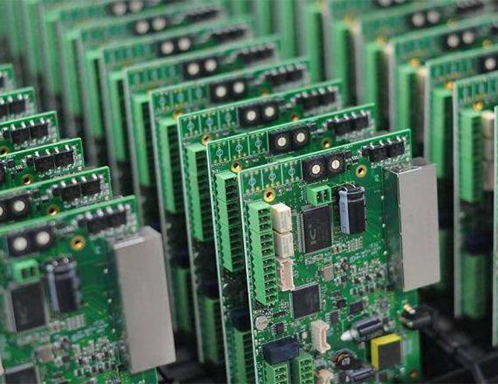
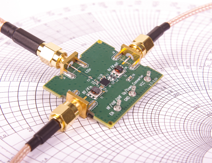
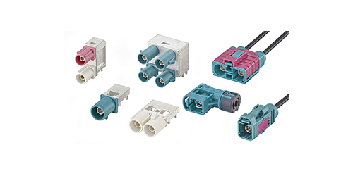
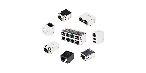
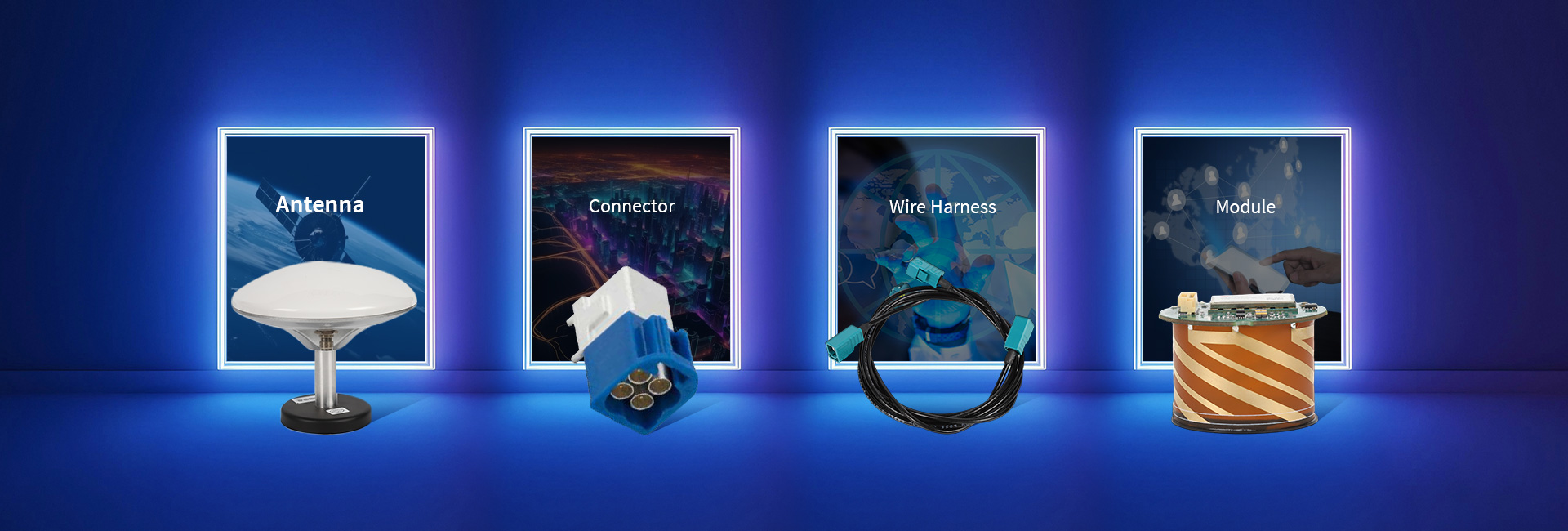
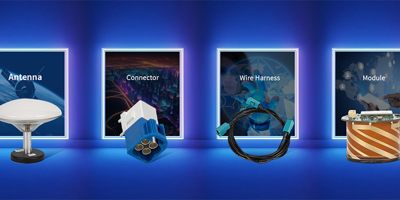
Products -PCBA Manufacturing RF Connectors RF Cable Assemblys Embedded Antennas External Antennas Positioning Chips and Modules
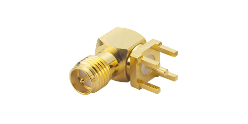
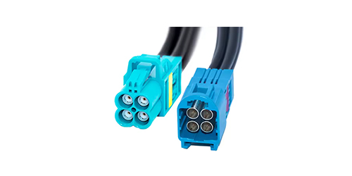
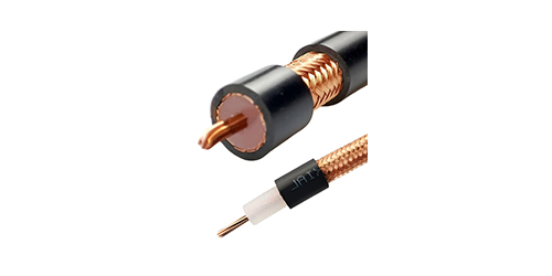
RF Connectors

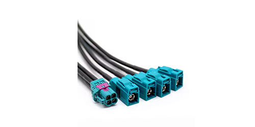
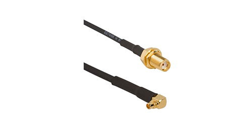
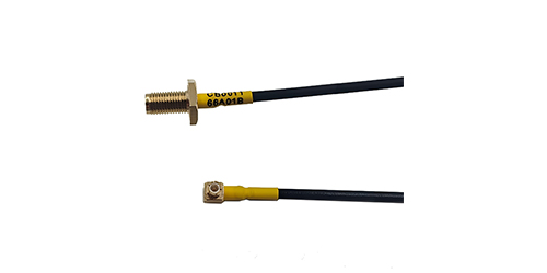
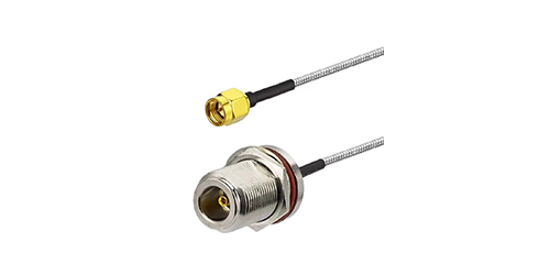
RF Cable Assemblys
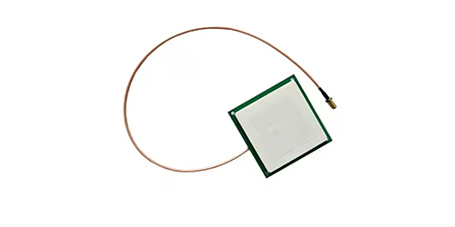
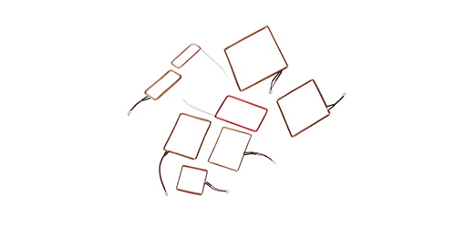
Embedded Antennas
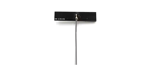
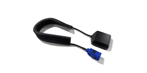
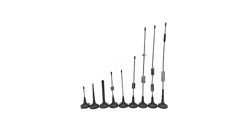
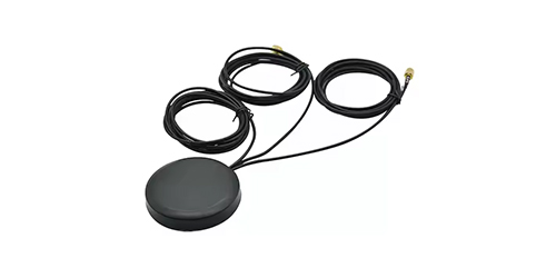
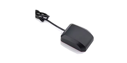
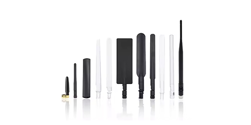
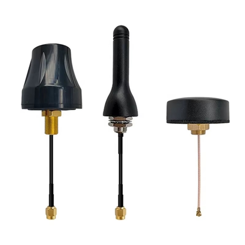
External Antennas
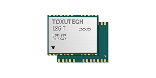
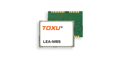
Positioning Chips and Modules
 Language


Language

In the relentless pursuit of smaller, faster, and more connected electronic devices, the antenna has consistently posed a significant engineering challenge. It is the critical gateway between the digital world and the electromagnetic spectrum, yet its physical properties often seem at odds with the goals of miniaturization and sleek design. The High-Performance Low-Profile Ceramic Antenna represents a definitive solution to this paradox, embodying a remarkable convergence of advanced materials science, electromagnetic engineering, and precision manufacturing to deliver exceptional wireless performance in an ultra-compact form factor.
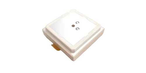
A High-Performance Low-Profile Ceramic Antenna is a type of embedded antenna characterized by its exceptional electrical capabilities and minimal spatial footprint. Its name reveals its core attributes:
High-Performance: This signifies metrics that far exceed those of basic antennas: wide bandwidth covering multiple frequency bands, high radiation efficiency (>60-70%), stable gain across its operating range, and a well-defined, stable phase center. This performance is comparable to larger external antennas but is achieved within a miniature package.
Low-Profile: The antenna has an extremely small vertical height, typically ranging from 1mm to 4mm. This allows it to be integrated into devices where z-height is a critical constraint, such as smartphones, wearables, ultra-thin laptops, and modular IoT sensors, without requiring a protruding housing.
Ceramic: The antenna's core is a block of ceramic material with a very high dielectric constant (εr). This is the key to its miniaturization, as it allows the antenna to be electrically large (resonant at target frequencies) while being physically very small.
The driving force behind this technology is the explosion of modern consumer and industrial electronics. The transition to 5G, the proliferation of Internet of Things (IoT) devices, the advent of ubiquitous autonomous systems, and the consumer demand for ever-thinner gadgets have created a environment where internal real estate is at a premium. Designers can no longer afford to dedicate large areas of a PCB to antenna traces or allocate space for bulky external antennas. The antenna must become invisible, seamlessly integrated into the device's form factor without compromising the wireless connectivity that users demand.
However, achieving "high performance" in a "low-profile" design is a profound engineering challenge. Fundamental electromagnetic principles dictate trade-offs between size, bandwidth, and efficiency. Shrinking an antenna typically narrows its bandwidth and reduces its efficiency. Therefore, creating a antenna that is both small and capable requires innovative approaches that bend these traditional rules. This involves sophisticated multi-resonant structures, novel ceramic compositions, and a deep, system-level understanding of the antenna's interaction with its host device.
These antennas are not mere commodities; they are highly engineered components. They are found in the most advanced smartphones enabling robust 5G and Wi-Fi 6E connectivity, in precision GPS modules for drones, in wearable health monitors that require reliable data transmission, and in the myriad of industrial sensors that form the backbone of Industry 4.0. They represent the silent enablers of the wireless world, providing the critical link that allows devices to communicate, navigate, and sense their environment, all while remaining hidden from view. This overview sets the stage for understanding the intricate design, operational principles, and nuanced trade-offs that define this pinnacle of miniaturized RF technology.
The design and construction of a high-performance low-profile ceramic antenna is a meticulous process that blends materials science, electromagnetic theory, and precision engineering. It is a deliberate departure from traditional antenna designs, employing specialized techniques to overcome the inherent limitations of a small form factor.
1. The Ceramic Core: The Foundation of Miniaturization
The heart of the antenna is a sintered ceramic block, typically composed of a titanium-based compound (e.g., Barium Strontium Titanate). The single most important property of this ceramic is its very high dielectric constant (εr or Dk), which can range from 20 to over 90. A high Dk is the fundamental enabler of miniaturization. The physical length required for an antenna to resonate at a specific frequency is inversely proportional to the square root of the Dk (λ = λ₀ / √εr). By using an ultra-high-Dk material, the wavelength within the ceramic is dramatically shortened, allowing the physical antenna size to be reduced to a small fraction of the free-space wavelength. For example, a ¼ wave antenna at 2.4 GHz can be shrunk from about 31 mm to just 3-5 mm.
2. The Radiating Element: Advanced Structures for Wideband Performance
The radiating element is a precision-patterned conductive material, usually silver or copper, printed onto the ceramic surface. To achieve high performance (wide bandwidth) in a small size, simple designs are insufficient.
Stacked-Patch Configuration: This is a common technique for multi-band operation. Multiple ceramic layers are used, each with a patch of a different size. A larger patch is tuned to a lower frequency band (e.g., GPS L1 at 1575 MHz), while a smaller patch on a layer above is tuned to a higher frequency band (e.g., 5G n77 at 3.5 GHz). The patches are electromagnetically coupled, allowing a single feed point to excite resonances across multiple bands.
Coupled-Feed and Slot-Loaded Designs: Instead of directly feeding the patch, engineers use coupling from a microstrip line beneath or adjacent to the patch. Alternatively, slots can be cut into the patch to create additional resonant paths. These techniques provide more degrees of freedom to control the impedance bandwidth and achieve better matching across a wider frequency range.
3. The Feed Network: Precision Impedance Matching
The feed network is the critical circuit that transfers energy from the antenna element to the transmitter/receiver IC. Its design is paramount for achieving a good impedance match (close to 50 ohms) across all desired bands. In a low-profile antenna, this network is often designed directly into the ceramic substrate or onto the attached PCB. It must be meticulously optimized using 3D electromagnetic simulation software to account for the effects of the ceramic material and the proximity of the device's ground plane.
4. The Role of the Ground Plane
A low-profile ceramic antenna is not a standalone component. Its performance is intrinsically linked to the PCB's ground plane of the host device. The antenna element excites currents on this ground plane, which itself becomes a significant part of the radiating system. The size and shape of this ground plane are critical design parameters. Manufacturers provide strict guidelines on the minimum required ground plane area and its keep-out regions. An undersized or poorly designed ground plane will detune the antenna, drastically reducing its efficiency and bandwidth.
5. Advanced Materials and Fabrication
Low-Loss Ceramics: High-performance antennas use ceramics with not only a high Dk but also a very low loss tangent. This ensures that more of the energy is radiated into space rather than being dissipated as heat within the material itself, directly translating to higher radiation efficiency.
Precision Manufacturing: The manufacturing process involves printing electrodes onto ceramic sheets, laminating them under high pressure and temperature, and then firing them in a kiln. The layers must be perfectly aligned, and the dimensions must be held to tight tolerances (often within microns) to ensure consistent performance across mass production.
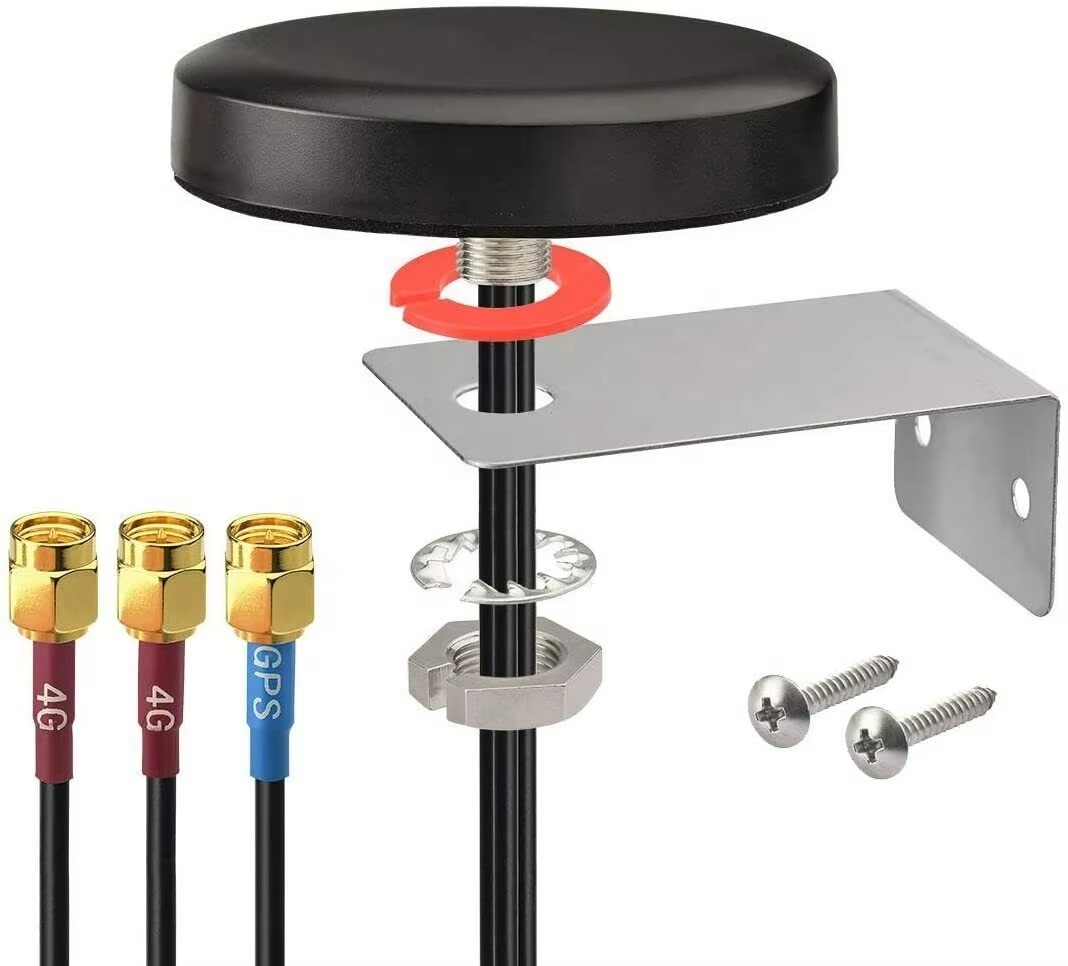
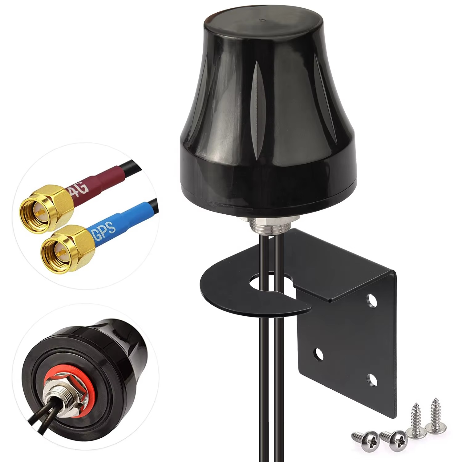
6. Packaging and Integration
The final antenna is packaged as a Surface-Mount Device (SMD). The solder pads are designed to create a precise stand-off height, resulting in a small air gap between the antenna body and the PCB after reflow soldering. This air gap is a critical part of the designed operating environment, as its lower dielectric constant (~1) compared to the PCB's FR4 substrate (~4.4) is essential for achieving the desired bandwidth and efficiency.
In summary, the construction of a high-performance low-profile antenna is a holistic process. It results in a component that is intentionally designed to be part of a larger system. Its exceptional performance is co-designed with the host device's PCB, making the system integrator a crucial partner in realizing the antenna's full potential.
The operation of a high-performance low-profile ceramic antenna is a sophisticated process that leverages the unique properties of its materials and structure to overcome the limitations of its size. It functions not as a simple resonator but as a highly efficient transducer and impedance transformer.
1. Dielectric Resonance: The Core Mechanism
The primary working principle is dielectric resonance. Unlike a wire antenna that resonates based on its physical length, the ceramic antenna resonates based on the wavelength within the high-dielectric material. The electromagnetic waves are effectively "slowed down" and concentrated within the ceramic block. This allows the physical structure to be much smaller than the free-space wavelength while still achieving electrical resonance at the desired frequency (e.g., 2.4 GHz or 5 GHz). The dimensions of the ceramic block and the patch electrode are meticulously calculated to excite specific resonant modes within the dielectric material.
2. Multi-Resonance for Wide Bandwidth
A single resonant mode produces a narrow bandwidth. To achieve the wide bandwidth required for high-performance applications (e.g., covering the entire 5 GHz Wi-Fi band from 5.15 to 5.85 GHz), the antenna is designed to support multiple, closely-spaced resonant modes.
Stacked Patches: In a multi-layer design, the different patches resonate at different frequencies. The coupling between these patches merges their individual bandwidths into a single, continuous wide bandwidth.
Slot and Feed Coupling: Introducing slots in the patch or using coupled feeds excites additional modes. The art of design is to position these resonances so that they overlap, creating a smooth and broad impedance bandwidth that can sometimes exceed 20% of the center frequency.
3. The Symphony with the Ground Plane
The antenna does not operate in isolation. The currents on the ceramic radiating element induce "image currents" on the PCB's ground plane. These currents cause the entire ground plane to radiate. Therefore, the complete, functional antenna system is the combination of the ceramic chip and the PCB ground plane. The antenna element acts as an "exciter," efficiently transferring energy to the larger ground plane, which then radiates it effectively. This partnership is crucial for achieving reasonable gain and efficiency from such a small component.
4. Controlled Radiation Pattern
The combination of the ceramic element and the ground plane shapes a specific radiation pattern. For a typical patch antenna mounted near the edge of a PCB, the pattern is directional. It has maximum gain broadside to the patch (perpendicular to the PCB) and reduced gain towards the plane of the board. This is often desirable, as it directs energy away from the lossy components and the user's body, towards the external environment where the router or base station is located.
5. Impedance Matching: The Critical Handshake
For maximum power transfer, the impedance of the complete antenna system must match the 50-ohm standard of the RF circuitry. This is incredibly challenging for a small, wideband antenna. A sophisticated matching network—a circuit of capacitors and inductors placed on the PCB between the antenna feed and the transceiver—is absolutely mandatory. This network transforms the antenna's complex impedance to as close to 50 ohms as possible across the entire band. The design of this network is not generic; it must be customized for the final PCB layout using a vector network analyzer (VNA).
6. Maintaining Efficiency
The goal is to maximize radiation efficiency—the percentage of power accepted at the terminals that is actually radiated. Losses are mitigated by:
Using low-loss-tangent ceramic.
Ensuring high conductivity in the electrodes (using silver).
Designing a effective ground plane.
Optimizing the matching network to minimize reflected power.
A well-designed implementation can achieve radiation efficiencies of 60-80% (-2.2 to -1 dB), which is exceptional for such a small form factor.
In essence, the antenna works by acting as a highly efficient, multi-resonant coupler. It concentrates electromagnetic energy within its small volume and efficiently transfers that energy to the PCB's ground plane, which then launches it into free space with a controlled pattern and wide bandwidth, enabling robust wireless communication.
The high-performance low-profile ceramic antenna offers a transformative set of advantages for modern product design, but these benefits are counterbalanced by significant technical challenges that demand expert engineering to overcome.
Advantages:
Extreme Miniaturization and Design Freedom: This is the paramount advantage. Its tiny form factor and low profile liberate industrial designers, allowing them to create sleek, compact devices without being constrained by antenna protrusions or large PCB keep-out areas. It enables the design of ultra-thin smartphones, compact wearables, and miniaturized IoT sensors.
High Performance in a Small Package: It delivers performance (bandwidth, efficiency) that was previously only achievable with much larger antennas. This includes support for complex multi-band and MIMO (Multiple-Input, Multiple-Output) configurations essential for 5G and Wi-Fi 6/6E.
Excellent Reliability and Consistency: As a single, solid ceramic component soldered directly to the PCB, it is highly resistant to shock, vibration, and physical wear. The SMD manufacturing process ensures consistent performance across high-volume production runs.
Simplified RF Design (to a point): The antenna is provided as a pre-characterized component. While integration is complex, the designer does not have to design the radiating element from scratch, as they might with a PCB trace antenna.
Good Immunity to Environmental Detuning: Once installed and potted, the antenna is less susceptible to detuning from the device's plastic casing or nearby objects compared to some other embedded antenna types, due to the concentrating effect of the high-Dk ceramic.
Challenges:
Performance Deeply Dependent on Integration: This is the greatest challenge. The antenna's performance is not intrinsic; it is a product of its integration. The PCB layout, ground plane size and shape, component placement, and plastic housing all dramatically affect its efficiency, bandwidth, and resonance. RF expertise is absolutely mandatory for success.
Narrower Bandwidth and Efficiency Trade-offs: Despite advanced designs, physics still imposes limits. Achieving ultra-wide bandwidth (e.g., to cover from 600 MHz to 6 GHz) in a single, very small antenna remains extremely challenging and often requires trade-offs in efficiency.
Sensitivity to the Human Body (Hand Effect): The human body is mostly water, which has a high dielectric constant and is lossy. When a hand grips a device, it can detune the antenna's resonant frequency, block its radiation pattern, and drastically reduce its efficiency. This is a major design hurdle for handheld devices.
Complex and Expertise-Driven Design Process: Successfully integrating one of these antennas is a specialized task requiring:
Careful PCB Stack-up Design: Ensuring continuous ground planes.
Strategic Placement: Locating the antenna in a optimal position, often at the edge of the board, away from noise sources and large obstructive components like batteries and displays.
Mandatory Tuning and Validation: The matching network must be optimized on the final physical board with its enclosure installed. This requires access to a vector network analyzer (VNA), an anechoic chamber, or a reverberation chamber for OTA (Over-the-Air) testing, and significant RF engineering knowledge.
Cost: High-performance ceramics with low loss tangents and the complex multi-layer manufacturing process make these antennas more expensive than simple PCB trace antennas or lower-grade ceramic chips.
Susceptibility to PCB Noise: Located on the main PCB, the antenna is vulnerable to noise from digital circuits (processors, memory), switching power supplies, and other co-located radios. Careful board layout, strategic shielding, and effective filtering are essential.
In conclusion, the advantages of small size and high performance make these antennas essential for cutting-edge consumer electronics. However, these benefits are exchanged for a set of complex design challenges that require specialized knowledge and careful system-level design to overcome. The component cost is often overshadowed by the high engineering cost of proper integration.
The high-performance low-profile ceramic antenna is the key enabling technology for a new generation of compact, connected, and intelligent devices. Its applications are found wherever advanced wireless functionality must be packed into a minimal volume.
Applications:
Smartphones and Tablets: This is the primary driver. These antennas are used for every wireless function: 5G sub-6 GHz, Wi-Fi 6/6E, Bluetooth, GPS, and UWB (Ultra-Wideband). Multiple antennas are used in MIMO arrays to achieve high data rates and spatial diversity.
Wearable Technology: Smartwatches, fitness trackers, and AR/VR glasses have extreme space constraints. Low-profile antennas are essential for providing robust Bluetooth and Wi-Fi connectivity in these tiny form factors.
Ultraportable PCs and Laptops: The drive for thinner and lighter laptops necessitates the use of these antennas for Wi-Fi, Bluetooth, and cellular connectivity, often in a MIMO configuration for better performance.
Internet of Things (IoT) Modules and Sensors: Compact IoT modules for industrial monitoring, asset tracking, and smart home devices use these antennas to provide reliable cellular (LTE-M, NB-IoT), Wi-Fi, or LoRaWAN connectivity in a small package.
Drones and Robotics: Small drones and robotic platforms require reliable command-and-control links (Wi-Fi, proprietary radio) and precise GPS positioning. Low-profile antennas are ideal due to their small size and weight.
Automotive Telematics: Used in telematics control units (TCUs) for connected car services, providing GPS and cellular connectivity in a package that can be easily integrated into the vehicle's design.
Future Trends:
Antenna-in-Package (AiP) and Antenna-on-Chip (AoC): The ultimate step in integration is to embed the antenna directly into the package of the RF system-on-chip (SoC) or even on the silicon die itself. This will save PCB space but presents immense challenges in isolating the antenna from the noise of the silicon.
Reconfigurable Intelligent Surfaces (RIS): Moving beyond static antennas, future devices may have surfaces that can dynamically change their electromagnetic properties to optimize signal reception and transmission in real-time, mitigating the hand effect and blocking.
AI-Enhanced Design and Optimization: Machine learning algorithms will be used to rapidly simulate and optimize antenna designs and their integration, dramatically reducing design cycles and helping to find non-intuitive solutions for better performance.
Tighter Integration with Metamaterials: The use of engineered metamaterials could allow for even greater levels of miniaturization or for creating effective ground planes in smaller areas, breaking traditional size limitations.
Higher Frequency Support (mmWave): While different in design, the principles of integration will be pushed further to incorporate mmWave antenna arrays for 5G and beyond into compact modules, complete with beamforming capabilities.
Multi-Functional Antennas: A single antenna element designed to operate at vastly different frequency bands for completely different services (e.g., 5G and satellite messaging) will be a key area of research.
The future of this antenna is one of even deeper integration, greater intelligence, and more complex functionality, continuing to be the hidden enabler of the wireless world.
Conclusion
The high-performance low-profile ceramic antenna is a masterpiece of modern engineering. It is a component that embodies the relentless industry trend of doing more with less: delivering the complex, wideband, multi-protocol connectivity required by today's devices from a package so small it is effectively invisible. Its development is a critical enabler that has allowed the form factors of our most beloved gadgets to evolve without sacrificing—and indeed, while enhancing—their wireless capabilities.
Its value is immense. By decoupling antenna performance from physical size, it has become the cornerstone of the smartphone revolution, the enabler of wearable computing, and the key to miniaturized IoT. It has allowed technology to recede into the background, becoming seamlessly integrated into the objects we use every day. This is no small feat; it represents a fundamental triumph over one of the most stubborn physical constraints in electronics.
However, this capability comes with a caveat of complexity. This antenna is a demanding partner in the design process. Its successful integration is a testament to skilled RF design, requiring a deep understanding of the interplay between the component, the PCB, and the device's ecosystem. It punishes poor design with dismal performance but rewards meticulous engineering with remarkable capability. It teaches a critical lesson: in modern electronics, the line between a component and a system is often blurred.
The future of this technology is bright and必然 (bìrán - inevitable). As materials improve, integration deepens, and design tools become more sophisticated, we can expect these antennas to become even smaller, more efficient, and more resilient to their operating environment. They will be the hidden engines of the next generation of connectivity, from the metaverse to the autonomous IoT. The high-performance low-profile ceramic antenna is far more than a simple receiver; it is a gateway to a more connected and efficient future, proving that the most powerful capabilities can indeed come in the smallest of packages.

 86 0755 2819 9597
Lucy Yang | lucy.y@toxutech.com
Nicole Li | nicole@toxutech.com
Dotty Zhao | sales04@toxutech.com
Global Business Director / Sales Team / Global Operations


 En
En Cn
Cn Korean
 Home >


