

-
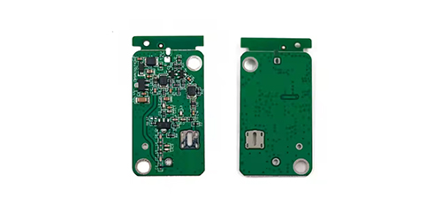
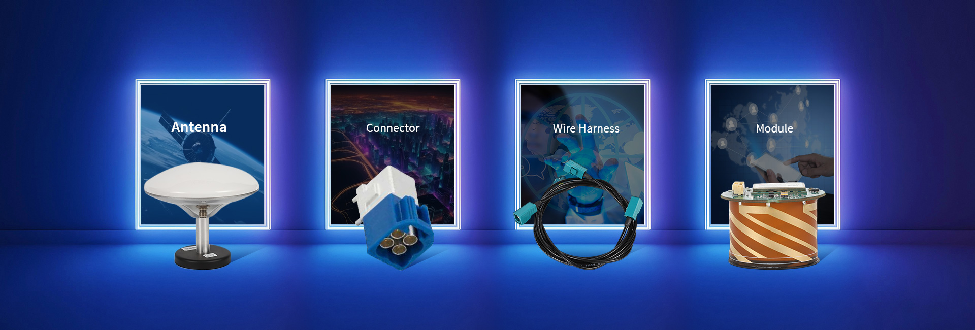
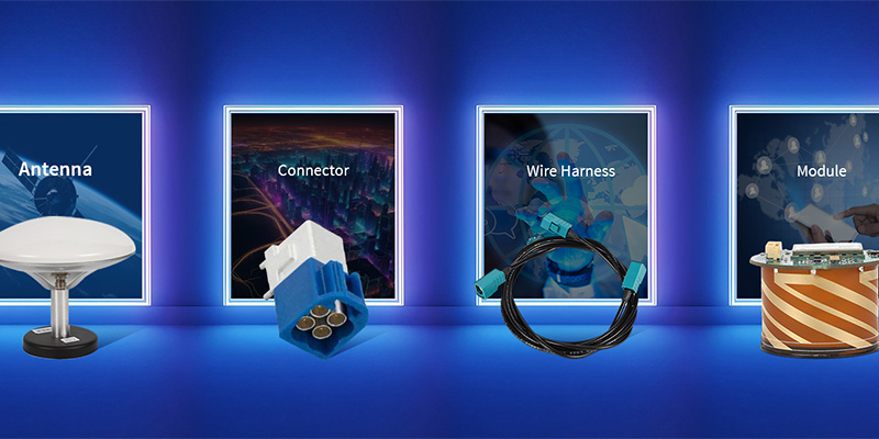
Products -PCBA Manufacturing RF Connectors RF Cable Assemblys Embedded Antennas External Antennas Positioning Chips and Modules
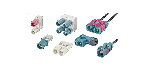
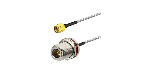
RF Connectors

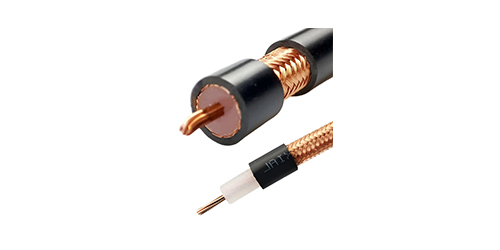
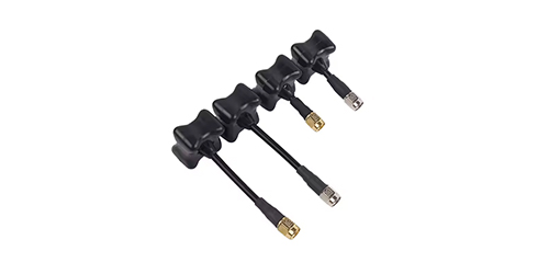
RF Cable Assemblys
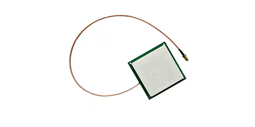
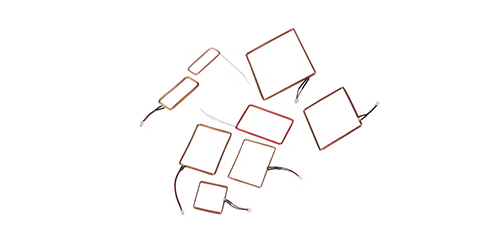
Embedded Antennas
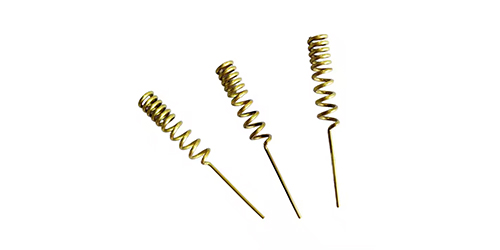
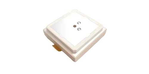
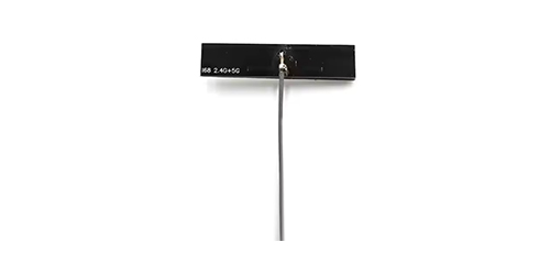
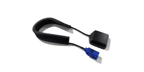
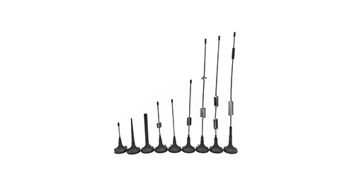
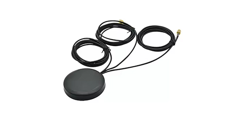
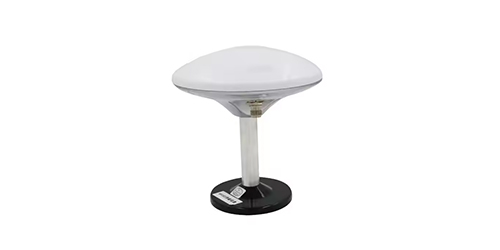
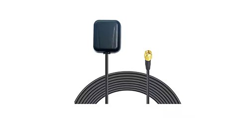
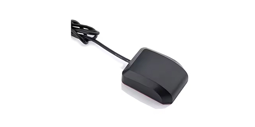
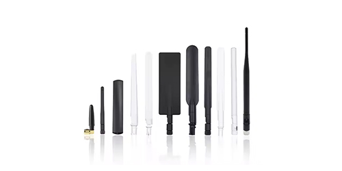
External Antennas
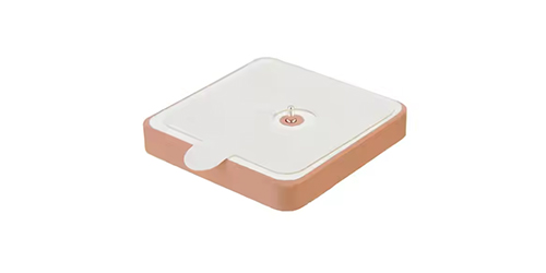
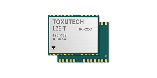
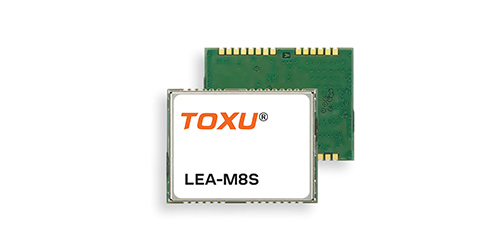
Positioning Chips and Modules


 Language


Language

In the intricate ecosystem of modern electronics, the ability to know one's precise location on Earth has evolved from a luxury to a fundamental expectation. This capability is powered by Global Navigation Satellite Systems (GNSS), a network of constellations including GPS (USA), GLONASS (Russia), Galileo (EU), and BeiDou (China). While the complex algorithms running on the receiver chip are often credited, the journey of a satellite signal begins at a single, critical component: the antenna. Among the various types, the embedded passive GNSS ceramic antenna has emerged as the dominant solution for integrating ubiquitous, low-cost positioning into a vast array of consumer and industrial devices.
.
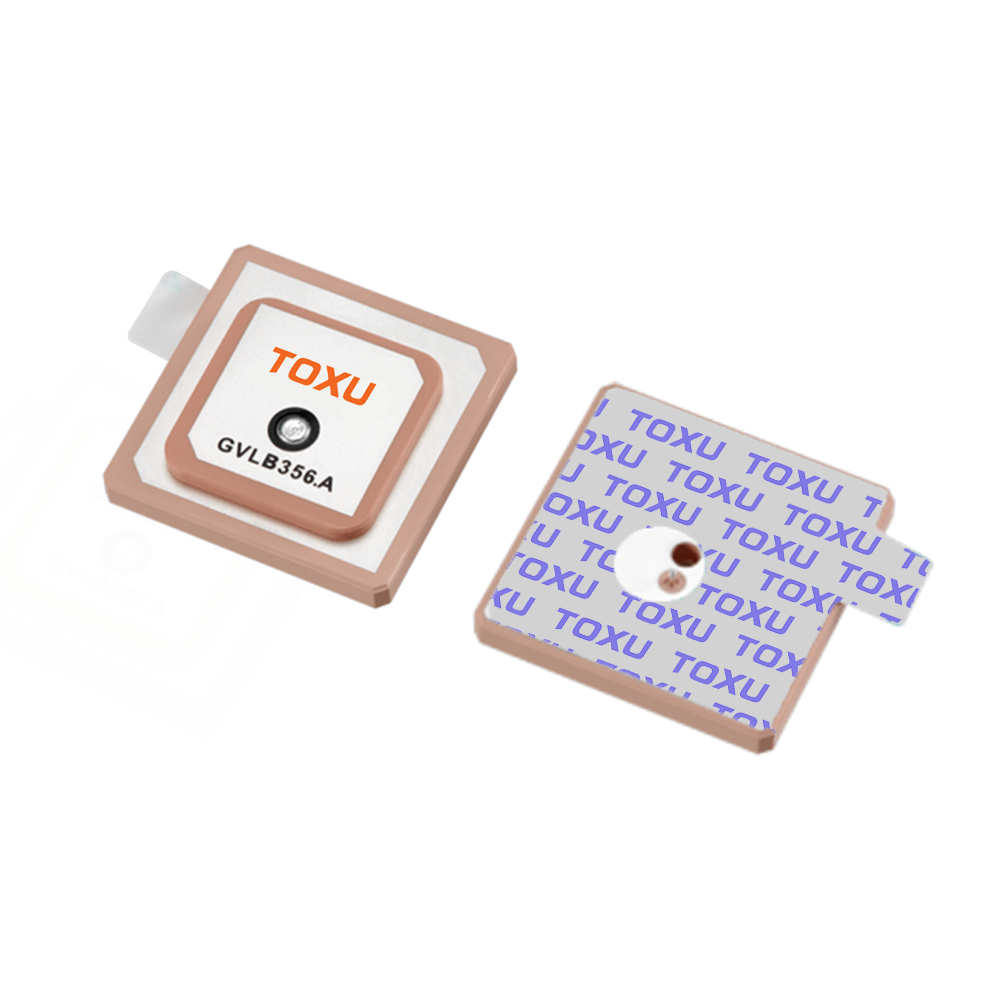
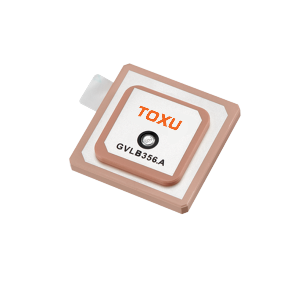
An embedded passive GNSS ceramic antenna is a type of antenna defined by its form, function, and integration method:
Embedded: It is not an external accessory but is permanently mounted within the device's enclosure, typically directly onto its main printed circuit board (PCB). This approach is fundamental to achieving sleek, compact, and robust product designs.
Passive: It contains no active electronic components, such as a Low-Noise Amplifier (LNA). It is a purely passive radiating element that does not require a separate power source. This simplifies the design and reduces the bill of materials (BOM) cost but places a greater burden on the system design to compensate for signal loss.
Ceramic: The antenna's core is a block of specialized ceramic material characterized by a high dielectric constant (εr). This property is the key to miniaturization, as it allows the antenna to be electrically large (resonant at GNSS frequencies around 1.5 GHz) while being physically very small.
GNSS: It is primarily designed to receive signals in the L1 band (1560-1610 MHz), which is common to all major satellite constellations, providing broad compatibility.
The proliferation of this antenna technology is a direct consequence of the consumer electronics revolution. The demand for location capabilities in smartphones, wearables, drones, asset trackers, and Internet of Things (IoT) sensors necessitated an antenna solution that was inexpensive, tiny, reliable, and could be invisibly integrated during high-volume, automated manufacturing. Unlike external active antennas, which offer high performance but add cost, size, and assembly complexity, the embedded passive ceramic antenna prioritizes seamless integration and low cost, accepting a trade-off in ultimate performance.
However, the term "embedded" signifies a profound shift in design philosophy. An embedded antenna is not a standalone component whose performance is guaranteed by its datasheet. Instead, its functionality is co-designed by the device into which it is integrated. The PCB itself becomes a part of the antenna system. The size and shape of the board's ground plane, the placement of the antenna on it, the proximity of other components, and the material properties of the device's plastic casing all have a dramatic and often decisive impact on the antenna's efficiency, bandwidth, and radiation pattern. A poor implementation can render a well-designed antenna nearly useless, leading to weak signal reception, long time-to-first-fix (TTFF), and unreliable positioning.
Therefore, the embedded passive ceramic antenna represents a triumph of miniaturization and manufacturing efficiency, but it also demands a higher level of RF design discipline. It is the hidden engine, the silent conduit that connects our miniature electronic worlds to the vast constellation of satellites overhead, enabling the location-aware revolution from the palm of our hands.
The design and construction of an embedded passive GNSS ceramic antenna is a sophisticated exercise in electromagnetic engineering, materials science, and cost-optimized manufacturing. Every aspect is meticulously crafted to achieve reliable resonance and radiation within a minuscule, low-cost package that can withstand the rigors of automated assembly and daily use.
1. The Ceramic Core: The Foundation of Miniaturization
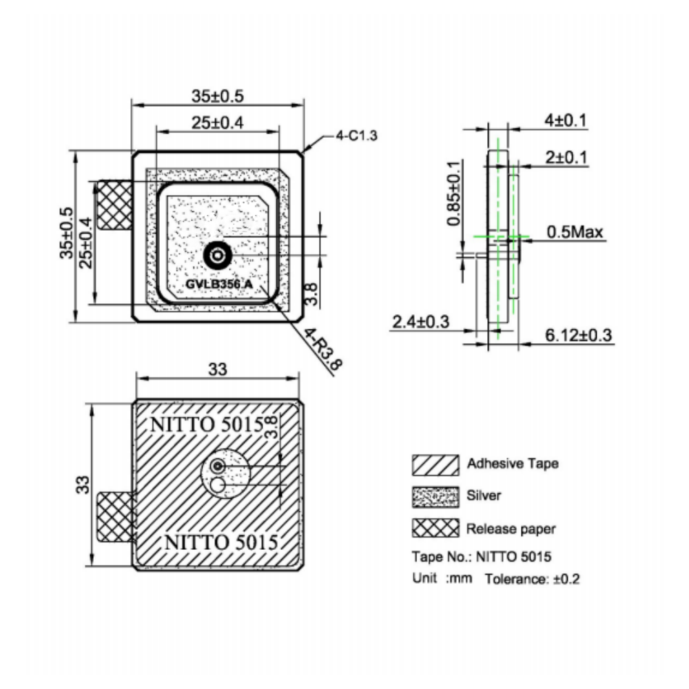
The heart of the antenna is a monolithic block of ceramic material, typically a composition based on titanium dioxide or other metal oxides. The single most critical property of this ceramic is its high dielectric constant (εr or Dk), which usually ranges from 20 to 40 for standard commercial antennas. This high Dk is the fundamental enabler of miniaturization. The physical length required for an antenna to resonate at a specific frequency is inversely proportional to the square root of the Dk (λ = λ₀ / √εr). By using a high-Dk material, the wavelength of the electromagnetic waves within the ceramic is dramatically shortened. This allows the physical antenna dimensions to be reduced to a small fraction of the free-space wavelength (approximately 19 cm for a quarter-wave at 1.5 GHz), resulting in typical form factors of 10x10x3 mm or even smaller.
2. The Radiating Element: Precision Electrodes
The radiating element is not a separate wire but a precisely patterned electrode, most commonly made from silver, that is printed, fired, and fused onto the surface of the ceramic block. The dominant design architecture is a variant of the Planar Inverted-F Antenna (PIFA). The PIFA is favored for its excellent compromise between size, bandwidth, and, crucially, its ease of impedance matching. Its key structural features include:
Radiating Plate: The main area of the electrode, whose dimensions primarily determine the resonant frequency.
Feed Point: The specific location where the signal is coupled to the RF transmission line on the host PCB via a solder pad.
Shorting Pin: A vital feature that electrically connects the radiating plate to the RF ground plane. This pin serves two key functions: it lowers the antenna's fundamental resonant frequency, allowing for further size reduction, and it helps to match the antenna's input impedance closer to the standard 50-ohm requirement of the GNSS receiver, simplifying the external matching network.
The exact geometry of this pattern is the result of extensive electromagnetic simulation and testing to optimize performance within the GNSS L1 band.
3. Materials and Cost-Optimized Manufacturing
The pursuit of low unit cost dictates material selection and production methodology:
Ceramic Composition: The specific ceramic blend is chosen for a balance of high Dk, adequate performance, and, most importantly, low cost and suitability for high-volume sintering processes. This often means accepting a higher loss tangent (a measure of signal energy dissipated as heat) compared to expensive aerospace-grade materials.
Electrode Fabrication: Silver paste is used due to its superb conductivity and compatibility with screen-printing and high-temperature co-firing processes.
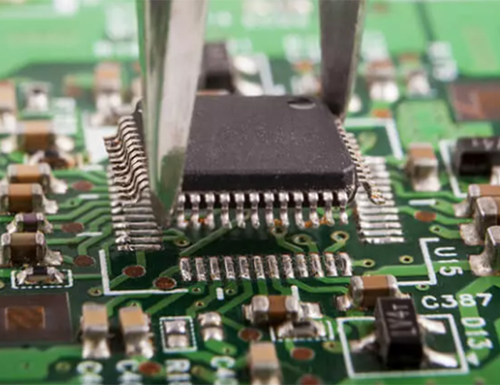
Mass Production: Manufacturing is highly automated for economies of scale. Large sheets of ceramic are printed with hundreds of electrode patterns, laminated, diced into individual units, fired in kilns, and then taped-and-reeled for use by automated pick-and-place machines. This scale is what drives the cost down to commodity levels.
4. The Indispensable Partner: The PCB Ground Plane
A critical and often misunderstood aspect of embedded antenna design is that the ceramic component is not a complete system. It is designed to function in concert with the PCB's ground plane, which becomes an integral and active part of the radiating structure. The currents on the ceramic element induce mirror currents on the ground plane, which itself radiates. Consequently, the size, shape, and integrity of this ground plane are paramount and often more influential on final performance than the antenna element itself. Manufacturers always specify a minimum required ground plane area (e.g., 40x40 mm or 70x25 mm) that must be kept clear of other components and signals. An undersized or fragmented ground plane is the most common cause of antenna failure.
5. SMD Packaging and Mounting
The antenna is packaged as a standard Surface-Mount Device (SMD). The solder pads on its underside are designed to create a precise standoff, resulting in a small air gap between the antenna body and the PCB after reflow soldering. This air gap, with its lower dielectric constant (~1) compared to the PCB's FR4 substrate (~4.4), is a crucial part of the antenna's designed operating environment. Soldering the entire base flat to the board would effectively embed it in the FR4, altering its dielectric environment, detuning its resonant frequency, and severely degrading its performance.
In summary, the construction of an embedded passive antenna is a holistic process of creating a "performance seed" that is intentionally designed to be incomplete. Its final characteristics are co-developed by the host device's PCB, making the system integrator a crucial partner in its performance. The design is a constant and delicate balance between achieving acceptable RF performance and hitting an aggressive cost target that enables mass-market adoption.
The operation of an embedded passive GNSS ceramic antenna is a delicate and intricate process of resonance, energy transfer, and environmental interaction. Its fundamental task is to efficiently capture infinitesimally weak electromagnetic energy from satellites over 20,000 kilometers away and deliver it as an electrical current to the receiver with minimal loss, all while being constrained within a hostile electronic environment.
1. Resonance: The Core Mechanism
At its heart, an antenna is a resonant structure. The ceramic PIFA is meticulously dimensioned to be electrically resonant at the center of the GNSS L1 frequency band (~1575.42 MHz). At resonance, the antenna's impedance is purely resistive (ideally 50 ohms) and its reactance is zero. This state allows for the maximum possible transfer of power from the incoming electromagnetic wave into the antenna's terminals. The high-dielectric ceramic material is essential for creating this resonance in a tiny physical space, as it effectively "slows down" the electromagnetic waves, reducing the required physical path length to achieve the necessary electrical length for resonance.
2. The Symphony with the Ground Plane
The antenna does not operate in isolation. The RF currents flowing on the ceramic radiating element induce corresponding "image currents" on the PCB's ground plane. These currents cause the entire ground plane to radiate. Therefore, the complete, functional antenna system is the combination of the ceramic chip and the PCB ground plane. The resulting radiation pattern is not a perfect sphere but is typically a misshapen hemisphere, directed preferentially away from the ground plane. This is often a beneficial trait, as it naturally directs energy toward the sky (where the satellites are) and away from the lossy components and batteries inside the device.
3. Impedance Matching: The Critical Handshake
For maximum power transfer, the impedance of the complete antenna system (ceramic element + ground plane) must match the impedance of the transmission line (the microstrip trace on the PCB) and the input impedance of the GNSS receiver, which is standardized at 50 ohms. While the PIFA's integrated shorting pin provides a good starting point, a perfect match is rarely achieved in practice due to the influence of the device's enclosure and other components. Therefore, an external matching network is almost always required.
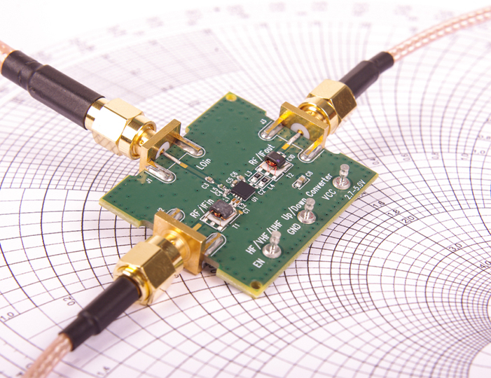
This network is a simple circuit of passive components—typically one or two capacitors and inductors—placed on the PCB between the antenna feed point and the receiver. This network's job is to transform the antenna's complex impedance to as close to a perfect 50-ohm match as possible. The design of this network is not generic; it must be customized and optimized for the final PCB layout and enclosure using a vector network analyzer (VNA). This tuning process is the single most important step in ensuring the antenna system performs to its potential.
4. Bandwidth: The Tightrope Walk
While individual GNSS signals are narrowband, the antenna needs sufficient bandwidth to cover the slight frequency variations between different constellations (all located within the 1560-1610 MHz L1 band) and to account for real-world perturbations. These include manufacturing tolerances, temperature changes, and the detuning effects of the plastic device casing. However, small antennas are inherently high-Q devices, which means they have a narrow bandwidth. antenna designers walk a tightrope, working to achieve an adequate bandwidth (typically 10-20 MHz) while maintaining high efficiency and a small form factor.
5. Efficiency: The Ultimate Measure of Success
The definitive metric for a passive antenna's performance is its radiation efficiency—the percentage of power accepted at its terminals that is actually radiated into space (or received from space). Efficiency is always less than 100% due to several loss mechanisms:
Dielectric Loss: Energy converted to heat within the lossy ceramic material.
Conductor Loss: Resistance in the silver electrodes.
Ground Plane Loss: Imperfect conduction in the PCB's copper.
Mismatch Loss: Power reflected back to the source due to impedance mismatch.
Near-Field Loss: Energy absorbed by nearby components (batteries, displays) and materials (the plastic housing).
A well-integrated embedded antenna might achieve 50-60% efficiency (-3 to -2.2 dB), meaning nearly half the signal is lost. A poor implementation can easily fall below 25% (-6 dB), crippling the receiver's ability to function reliably.
In essence, the antenna works by resonating in sympathy with the satellite signals. It captures their minuscule energy and, in concert with its ground plane, delivers that energy through a carefully tuned pathway to the receiver. The receiver's job is to amplify this weak signal and extract the data, but it can only work with what the antenna system provides. A weak, inefficient antenna forces the receiver to operate at the very edge of its sensitivity, resulting in poor performance, long acquisition times, and frequent signal drop-outs.
The decision to use an embedded passive GNSS ceramic antenna is a fundamental engineering compromise, offering a compelling set of advantages for modern product design while introducing a suite of significant technical challenges that must be meticulously managed to achieve success.
Advantages:
Extreme Miniaturization and Low Profile: This is the paramount advantage. Their tiny form factor (often under 100 mm³) allows them to be integrated into the most space-constrained devices like wearables, hearables, and compact IoT modules. This enables sleek, innovative product designs without external protrusions, cables, or connectors.
Very Low Unit Cost: Costing just pennies in high volume, this affordability is what makes GNSS functionality economically viable for consumer products and large-scale IoT deployments. It is a key enabler of the "location-aware everything" trend.
High Reliability and Ruggedness: As a single, solid ceramic component soldered directly to the PCB, it is highly resistant to shock, vibration, corrosion, and general wear and tear. There are no cables to break, connectors to become loose, or contacts to corrode, making it ideal for harsh environments and consumer products with long lifespans.
Simplified Assembly and Manufacturing: Being a standard SMD component, it is perfectly suited for fully automated PCB assembly using pick-and-place machines and reflow ovens. This eliminates manual assembly steps (like screwing on an external antenna), reduces manufacturing time and cost, and ensures consistent quality and placement accuracy across thousands of units.
Zero Power Consumption: As a purely passive component, it requires no power supply or bias tee circuitry. This simplifies the overall system design and contributes to lower total power consumption, which is critical for battery-operated devices.
Design Freedom and Aesthetics: It can be completely hidden within the device's enclosure, granting industrial designers complete freedom over the product's aesthetic form without being constrained by an external antenna element.
Challenges:
Performance Deeply Dependent on Integration: This is the single greatest challenge. The antenna's performance is not intrinsic; it is a product of its integration. The PCB layout, ground plane size and shape, component placement, and plastic housing all dramatically affect its efficiency, resonance, and bandwidth. A perfect antenna can be rendered useless by a poor PCB design, making RF expertise mandatory.
Inherently Lower Performance: Compared to an active external antenna with a clear view of the sky, an embedded passive antenna inherently has lower gain and efficiency due to its small size, higher-loss materials, and losses in the surrounding environment. This results in weaker signal reception, longer Time-To-First-Fix (TTFF), and significantly poorer performance in challenging signal environments like urban canyons, under dense tree cover, or indoors.
Severe Sensitivity to the Human Body (Hand Effect): The human body is mostly water, which is a very effective absorber of RF energy at GNSS frequencies. When a hand grips a device like a phone or watch, it can block the antenna's radiation pattern, detune its resonant frequency, and drastically reduce its efficiency by 10-20 dB or more. This is perhaps the most significant design hurdle for consumer devices.
Complex and Expertise-Driven Design Process: Successfully integrating one of these antennas is not a simple "drop-in" task. It requires significant RF expertise and involves:
Careful PCB Stack-up Design: Ensuring continuous, unbroken ground planes on the necessary layers.
Strategic Placement: Locating the antenna in a corner or at the edge of the board, away from noise sources and large obstructive components like batteries, displays, and cameras.
Mandatory Tuning and Validation: The matching network must be optimized on the final physical board with its enclosure installed. This requires access to a vector network analyzer (VNA), a GPS simulator or live-sky testing, and RF engineering knowledge.
High Susceptibility to PCB Noise: Located on the main PCB, the antenna is vulnerable to broadband noise generated by digital circuits (processors, memory, oscillators), switching power supplies, and other co-located radios (cellular, WiFi, Bluetooth). This noise can easily couple into the antenna and drown out the incredibly weak GNSS signals (which are below the noise floor), necessitating careful board layout, strategic shielding, and effective filtering.
Limited Bandwidth: It is challenging and expensive to design a very small, low-cost embedded antenna that covers multiple GNSS bands (e.g., L1 and L5) effectively. Most are optimized solely for the L1 band, limiting their use for high-precision applications that require multi-frequency operation.
In conclusion, the advantages of ultra-low cost, small size, and ruggedness make embedded passive ceramic antennas the default choice for mass-market electronics. However, these benefits are exchanged for a set of complex design challenges that require specialized knowledge and careful system-level design to overcome. The low component cost can often be offset by the higher engineering cost required for successful implementation.
The embedded passive GNSS ceramic antenna is the linchpin of the mass-market location revolution, finding its way into a breathtaking array of devices that define the modern connected world. Its future evolution is continuously shaped by the demands of these applications and the relentless push for better performance, deeper integration, and lower cost.
Applications:
Smartphones and Tablets: The primary driver of volume and innovation. Nearly every smartphone on the market uses one or more of these antennas for GNSS. Designers face a constant battle against space constraints, metal frames, large displays, and the detrimental "hand-effect" to provide reliable location services for navigation, geotagging, and countless apps.
Wearable Technology: Fitness trackers, smartwatches, and child monitors rely on these tiny antennas. This is arguably the most challenging environment due to extreme miniaturization and the significant signal blockage and detuning caused by the human body, which is often in direct contact with the device.
Asset Tracking and IoT: A massive and rapidly growing application area. Small, low-power trackers for logistics, supply chain management, agricultural monitoring, industrial sensing, and theft prevention use these antennas to report their position over cellular (LTE-M, NB-IoT), LoRaWAN, or other LPWAN networks.
Drones and Robotics: Consumer drones and small robotic platforms use these antennas for basic navigation, position holding, and return-to-home functions, where their small size, low weight, and ruggedness are critical advantages.
In-Vehicle Telematics and UBI: Small dongles that plug into a car's OBD-II port for usage-based insurance (UBI), fleet tracking, and diagnostic monitoring are classic applications, often leveraging the vehicle's exterior to get a better signal.
Consumer and Personal Electronics: Digital cameras (for geotagging photos), portable gaming devices, personal navigation devices (PNDs), and pet trackers have historically been major users.
GNSS Modules: Many off-the-shelf GNSS receiver modules for engineers and developers come with a pre-integrated and pre-tuned ceramic antenna, simplifying the design process for embedding GNSS into a final product.
Future Trends:
Improved Resilience to Detuning and Blocking: A major R&D focus is on designing antennas that are less sensitive to the effects of the human body and device casing. Advanced techniques include:
Reconfigurable and Tunable Antennas: Incorporating tunable components (like barium strontium titanate (BST) capacitors or varactor diodes) to dynamically adjust the antenna's resonance frequency and impedance matching in real-time as its environment changes (e.g., when a hand grips the phone). This actively compensates for detuning but adds cost and complexity.
Balanced (Differential) Feed Designs: Using a differential feed instead of a single-ended one can make the antenna less susceptible to near-field interference from the human body and other components.
Multi-Band Support for Mass Markets: As high-accuracy GNSS techniques (using L1 + L5 bands) trickle down from premium to mass-market applications, there is a growing need for low-cost embedded antennas that can operate efficiently across these widely separated bands. This is driving innovation in multi-resonant, coupled-element, and multi-layer designs.
Enhanced Integration and "Antenna-in-Package" (AiP): The next frontier in miniaturization is to move the antenna from the main PCB directly into the package of the GNSS receiver chip itself. AiP technology uses the package substrate to form the antenna, saving precious PCB space and simplifying system design. However, it presents immense challenges in isolating the antenna from the noise of the silicon die and achieving good efficiency.
Leveraging Device Elements: Using parts of the device itself—such as the metal frame, display bezel, or conductive coatings—as radiating elements to improve performance and efficiency, moving beyond the traditional ceramic block.
Advancements in Simulation and Modeling: More powerful and accessible electromagnetic (EM) simulation software (e.g., ANSYS HFSS, CST Studio) allows designers to accurately model the entire system—antenna, PCB, components, and housing—virtually before building physical prototypes. This reduces design cycles, cost, and risk of failure.
Material Science Innovations: Development of new ceramic and polymer-ceramic composite materials with lower loss tangents, more stable dielectric constants over temperature, and lower cost will enable better efficiency or smaller sizes.
The embedded passive ceramic antenna will remain the dominant solution for consumer GNSS for the foreseeable future. Its evolution will be characterized by incremental but critical improvements in bandwidth, stability, and integration depth, continuing to empower new and innovative location-aware applications across the globe.
Conclusion
The embedded passive GNSS ceramic antenna is a component of profound contradiction. It is both remarkably sophisticated and ruthlessly cost-optimized. It is ubiquitous yet invisible. It is the undeniable enabler of the modern location revolution, yet its success is entirely dependent on the design wisdom of the engineers who implement it. Its story is one of imperfection and indispensability, a testament to the engineering ethos of achieving "good enough" performance at a scale that changes the world.
Its most significant legacy is the democratization of precision. By reducing the cost and size of the GNSS entry point to mere pennies and millimeters, it has transformed a military-grade technology into a standard utility, as commonplace as the microcontroller itself. It has empowered a universe of applications, from guiding emergency services to tracking a food delivery order, from enabling autonomous farm equipment to helping a hiker find their way. This would simply not be possible with large, expensive, external antennas.
However, this accessibility comes with a stern caveat. The antenna's "low cost" and "easy assembly" are seductive traits that can mislead designers into underestimating the complexity of its integration. It is a component that punishes negligence and rewards expertise. Its performance is not a given; it is earned through careful system-level design, meticulous PCB layout, mandatory impedance tuning, and rigorous validation testing. The low component cost can be quickly eclipsed by the high engineering cost required to do it right.
The challenges it presents—sensitivity to environment, body detuning, lower efficiency, and noise susceptibility—are not design flaws but the direct and inevitable physical consequences of its microscopic size and minuscule cost. They are the fundamental trade-offs that define its existence. These very challenges are the forces that continue to drive innovation in materials science, electromagnetic simulation, and antenna design techniques, pushing the boundaries of what is possible within these constraints.
As we look toward a future of pervasive connectivity, autonomous systems, and an ever-expanding IoT, the demand for small, cheap, and reliable positioning will only intensify. The embedded passive ceramic antenna, continually evolving to become more robust, more wideband, and more intelligent, will remain at the heart of this evolution. It may never match the performance of its larger, active cousins, but it doesn't need to. Its job is to be good enough, everywhere, for everyone. It is a humble piece of ceramic, but it is the foundational gateway upon which our digitally located world is built.

 86 0755 2819 9597
Lucy Yang | lucy.y@toxutech.com
Nicole Li | nicole@toxutech.com
Dotty Zhao | sales04@toxutech.com
Global Business Director / Sales Team / Global Operations


 En
En Cn
Cn Korean
 Home >


