

-
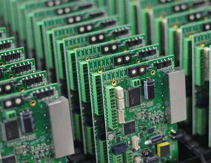
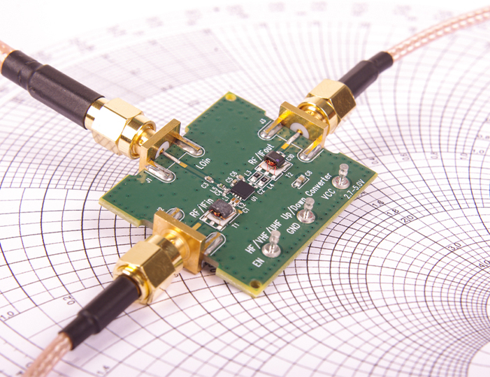
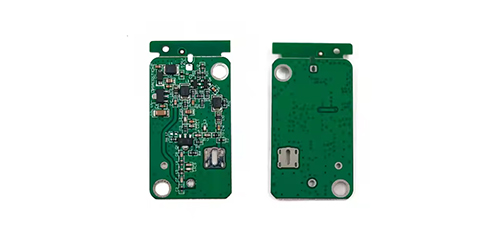
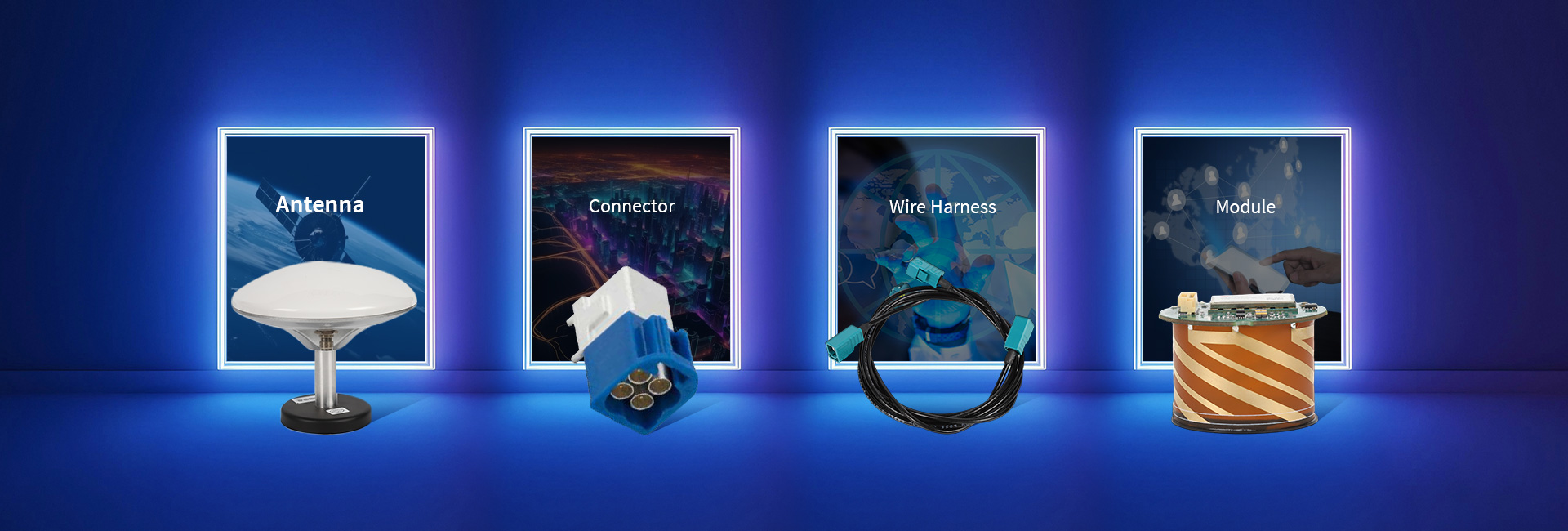
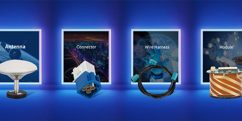
Products -PCBA Manufacturing RF Connectors RF Cable Assemblys Embedded Antennas External Antennas Positioning Chips and Modules
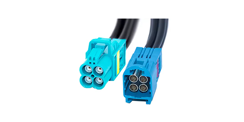
RF Connectors

RF Cable Assemblys
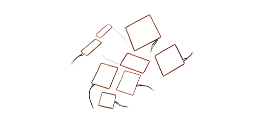
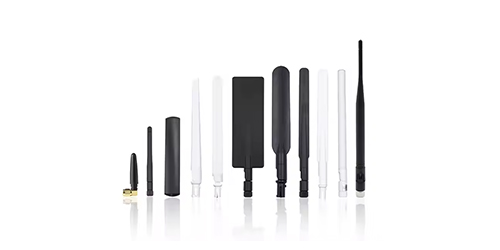
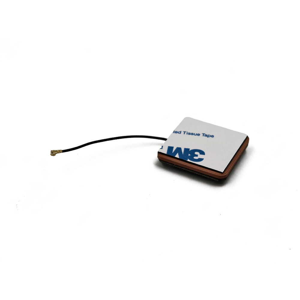
Embedded Antennas
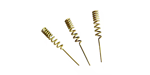
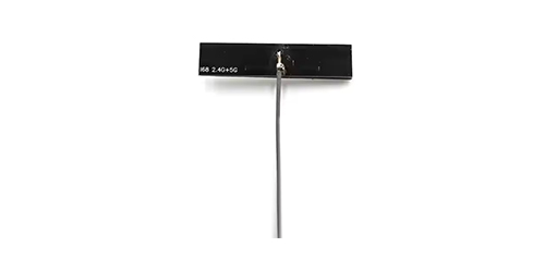
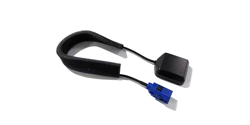
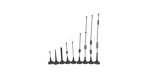
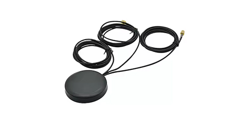
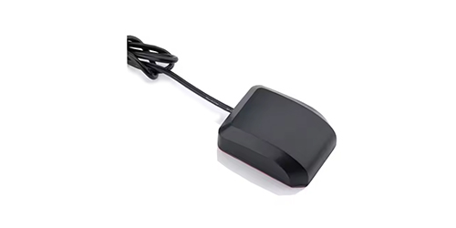
External Antennas
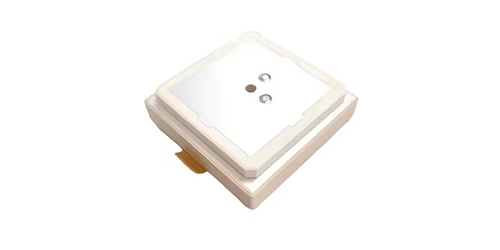
Positioning Chips and Modules
 Language


Language


The evolution of modern wireless communication systems—spanning from 5G and IoT to satellite networks and advanced radar—is fundamentally constrained by the performance and integration capabilities of their constituent components. At the heart of these systems lies the antenna, the critical transducer between guided electromagnetic waves within a circuit and free-space radiation. While passive antennas have served as the workhorse for decades, the relentless drive for miniaturization, enhanced functionality, and superior performance has catalyzed the development of a more sophisticated and integrated solution: the Active Ceramic Patch Antenna.
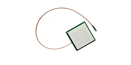
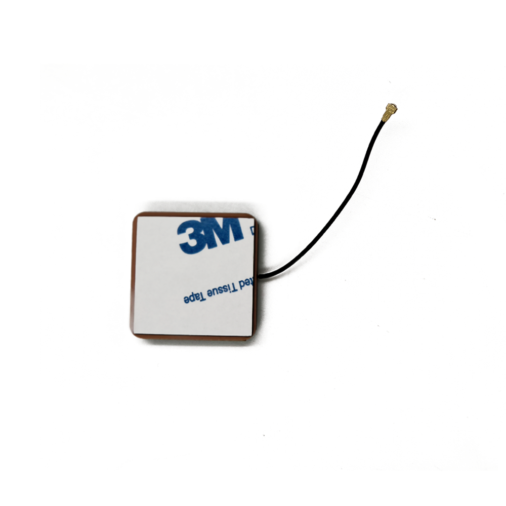
An Active Ceramic Patch Antenna is not merely an antenna; it is a complete, self-contained radio frequency (RF) front-end subsystem. The term "active" signifies the integration of semiconductor amplifying or processing circuits directly with the radiating element. "Ceramic" refers to the substrate material upon which the antenna patch and often the associated circuits are fabricated. This ceramic is not a simple insulator; it is a precisely engineered material with specific dielectric properties. Finally, "patch antenna" describes a type of microstrip antenna consisting of a flat, rectangular or circular conducting sheet (the patch) mounted over a larger ground plane.
The synergy of these elements creates a device that is far greater than the sum of its parts. Traditional systems involve a discrete passive antenna connected via a lossy transmission line (like coaxial cable) to separate external components such as low-noise amplifiers (LNAs), power amplifiers (PAs), filters, mixers, and even entire transceivers. Each interconnection introduces parasitic inductance, capacitance, signal loss, impedance mismatch, and vulnerability to external noise. The active ceramic patch antenna elegantly solves these issues by consolidating the antenna and key active electronics into a single, compact, surface-mountable package.
The historical context is crucial for appreciation. Patch antennas themselves gained prominence in the 1970s and 1980s due to their low profile, conformability, ease of fabrication using printed circuit board (PCB) technology, and low cost. However, they were often plagued by inherent limitations: narrow bandwidth, relatively low gain, and efficiency susceptible to the properties of the substrate material. Early substrates were standard PCB laminates like FR-4, which have high loss tangents, especially at higher frequencies, leading to significant signal dissipation as heat.
The introduction of high-performance ceramic materials, such as alumina (Al₂O₃), aluminum nitride (AlN), and most notably, low-temperature co-fired ceramic (LTCC) and high-temperature co-fired ceramic (HTCC), was a paradigm shift. These ceramics offer exceptional properties: low loss tangent (high efficiency), high dielectric constant (enabling miniaturization), superb thermal conductivity (dissipating heat from active components), and excellent mechanical stability. This made them an ideal foundation not just for the antenna, but for embedding intricate passive networks—resistors, capacitors, and inductors—within the substrate itself through multilayer fabrication processes.
The final evolutionary step was the "active" integration. Advances in semiconductor technology, particularly in Gallium Arsenide (GaAs) and Gallium Nitride (GaN) for RF applications, and the relentless miniaturization of silicon-based ICs (like RFCMOS), allowed for bare die or chip-scale packaged amplifiers, filters, and switches to be directly mounted onto or embedded within the ceramic substrate. This is achieved through techniques like wire bonding, flip-chip bonding, or fully integrated processes in LTCC. The result is a hermetically sealed, robust module that receives or transmits a signal with significantly enhanced performance.
The overarching significance of the active ceramic patch antenna lies in its role as an enabling technology for the next generation of wireless devices. It empowers designers to:
Shrink Form Factors: By integrating the entire RF front-end into a single package, devices like smartphones, IoT sensors, and satellite communicators can become smaller and sleeker.
Boost Performance: Eliminating interconnect losses and optimizing the impedance matching between the antenna and amplifier at the source dramatically improves system noise figure (on receive) and radiated power (on transmit).
Simplify Design and Assembly: For OEMs, using a pre-tuned, pre-matched module simplifies the complex RF design process, reduces time-to-market, and mitigates risks associated with high-frequency layout.
Enhance Reliability: The robust ceramic package protects sensitive components from environmental factors like moisture, dust, and mechanical shock, making it suitable for automotive, aerospace, and industrial applications.
In essence, the active ceramic patch antenna represents the culmination of trends in miniaturization, integration, and material science, transforming the antenna from a simple passive radiator into an intelligent, high-performance foundational element of modern wireless systems.
The design and construction of an active ceramic patch antenna is a sophisticated multidisciplinary endeavor, blending electromagnetics, semiconductor physics, thermal management, and advanced materials processing. It is a meticulous process of co-design, where the antenna element and the active electronics are not designed in isolation but are optimized as a single, synergistic system. The process can be broken down into several key stages: substrate selection, antenna element design, active circuit integration, thermal management, and packaging.
1. Substrate Selection and Material Science:
The choice of ceramic substrate is the first and most critical decision, as it dictates the electrical, thermal, and mechanical properties of the entire module.
Dielectric Constant (εr): A high dielectric constant (e.g., 6 to 40+ for ceramics vs. ~4.5 for FR-4) allows for a much smaller patch antenna size, as the wavelength within the material is reduced by a factor of √εr. This is the primary driver for miniaturization.
Loss Tangent (tan δ): This quantifies the signal loss within the substrate material. Ceramics like LTCC and alumina exhibit very low loss tangents (0.0001 to 0.002 at high frequencies), which is essential for maintaining high radiation efficiency. A low tan δ ensures that minimal RF energy is converted into wasteful heat within the substrate itself.
Thermal Conductivity (k): Active components generate heat. Ceramics like aluminum nitride (AlN) and beryllium oxide (BeO) have excellent thermal conductivity (150-300 W/mK), rivaling some metals, which allows them to efficiently draw heat away from power amplifiers and other heat-generating ICs, preventing thermal runaway and performance degradation.
Coefficient of Thermal Expansion (CTE): The CTE of the substrate must be closely matched to that of the semiconductor chips (e.g., silicon or GaAs) to prevent mechanical stress and cracking during temperature cycles, which is vital for long-term reliability.
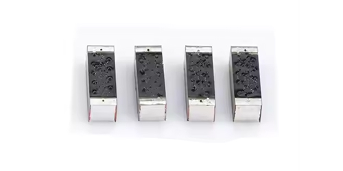
Common Materials: LTCC is overwhelmingly popular for complex modules. It involves printing metallic traces (e.g., silver, gold) onto unfired ("green") ceramic tape layers, stacking them, and then co-firing them in a furnace at around 850-900°C. This allows for the creation of embedded three-dimensional passive structures (resistors, capacitors, inductors, and transmission lines) within the substrate itself. HTCC (using alumina, fired at >1600°C) is more rigid and offers higher thermal conductivity but is less versatile for embedded passives. Alumina and Aluminum Nitride are often used as single-layer substrates for simpler, high-performance designs.
2. Antenna Element Design:
The patch itself is typically a thin, metallic (often copper or silver) film patterned on the top surface of the ceramic substrate. Its design is governed by fundamental equations, but heavily refined by electromagnetic simulation software (e.g., ANSYS HFSS, CST Studio).
Resonant Frequency: The primary dimension (length, L) of a rectangular patch is approximately half the wavelength in the dielectric medium (λg/2), which determines the resonant frequency. Sophisticated simulation is required to account for fringing fields, feed point location, and the effects of the surrounding package.
Feeding Techniques: How power is delivered to the patch is crucial. Common methods include:
Microstrip Line Feed: A direct conductor line from the active circuit to the patch edge. Simple but can radiate spuriiously.
Coaxial Probe Feed: A signal via drilled through the substrate from the ground plane to the patch. Provides good matching but is more complex to fabricate.
Aperture-Coupled Feed: The patch is on the top layer, and the feedline is on a buried layer, coupled through a slot in the intermediate ground plane. This provides excellent isolation between the antenna and the feed network.
Impedance Matching: The goal is to achieve a perfect 50-ohm match between the amplifier's output and the antenna's input port at the desired frequency. This is achieved by adjusting the feed point location, using matching stubs, or designing the feed network integrated within the LTCC layers. Perfect matching is easier to achieve in an integrated active antenna than in a discrete system.
3. Active Circuit Integration:
This is the defining feature of the "active" antenna. The RF integrated circuit (RFIC)—which could be a Low-Noise Amplifier (LNA) for receive, a Power Amplifier (PA) for transmit, a filter, a switch, or a complete transceiver—is integrated directly onto the ceramic substrate.
Bare Die Attachment: The semiconductor die (chip) is typically soldered or epoxied directly onto a pad on the ceramic surface. This minimizes parasitic package inductance.
Interconnection: Ultra-fine gold or aluminum wires are used in wire bonding to connect the pads on the die to the pads on the ceramic substrate. For higher-frequency performance, flip-chip bonding is used, where solder bumps on the die are directly attached to the substrate, minimizing interconnection length and inductance even further.
Embedded Components: In LTCC designs, passive components like bias tees, impedance matching networks, and DC blocking capacitors can be fabricated inside the substrate, saving surface area and improving performance.
4. Thermal Management and Packaging:
The ceramic substrate itself acts as the primary heat spreader. For high-power applications, the base of the ceramic module is often attached to a larger metal heat sink or the device's chassis using thermally conductive epoxy. The entire assembly is frequently encased in a protective plastic overmold or a metal lid to shield it from physical damage and environmental contaminants, resulting in a robust, surface-mount device (SMD) ready for automated PCB assembly.
The entire construction process is a careful balance of electrical performance, thermal dissipation, mechanical robustness, and manufacturability. The co-design philosophy ensures that the radiation characteristics of the patch are not adversely affected by the nearby active components and vice-versa, resulting in a highly optimized and performant RF module.
Understanding the working principle of an active ceramic patch antenna requires dissecting its operation into two primary modes: transmission and reception. The core physics of the patch antenna remains unchanged, but its performance is profoundly augmented by the intimate integration of active electronics.
Fundamental Radiation Mechanism of the Patch:
A basic patch antenna operates as a resonant cavity. The patch conductor and the larger ground plane beneath it form two parallel plates. The length L of the patch is carefully designed to be approximately half of the wavelength of the desired radio wave within the dielectric substrate (λ_g = λ_0 / √ε_r, where ε_r is the substrate's dielectric constant). When RF power is fed to the patch (e.g., at its edge or via a probe), it excites a standing wave of electric current on the patch. The strongest currents flow at the resonant frequency.
The key to radiation lies in the fringing fields at the edges of the patch. The electric field lines originate from the patch, arc through the air above, and terminate on the ground plane. These fringing fields are not entirely confined and are able to propagate energy into free space. The two radiating edges (along the length L) act like two radiating slots, which are the primary sources of radiation. The pattern is typically broadside, meaning maximum radiation is perpendicular to the plane of the patch.
Active Transmission Mode:
In a traditional system, a power amplifier (PA) is located on a main board, and its output is routed via a PCB trace and a connector to a cable, which then connects to a passive antenna. Each stage introduces loss.
In an active transmit antenna, the PA die is mounted directly onto the ceramic substrate, very close to the feed point of the patch.
The output of the PA is connected to the patch via a short wire bond or flip-chip bump and an impedance-matching network that is co-designed with the antenna. This matching network is often implemented as part of the LTCC layers.
The PA amplifies the intermediate frequency (IF) or RF signal from the transceiver chip. This amplified RF signal is delivered to the patch with minimal loss because the interconnect is extremely short and optimized.
The patch then radiates this powerful signal efficiently. The integration ensures that the PA sees a stable, well-matched load (the antenna), which is crucial for its linearity and efficiency. The excellent thermal conductivity of the ceramic substrate draws heat away from the PA, allowing it to operate at higher power levels reliably.
Active Reception Mode:
This is where the benefits are perhaps most dramatic. A fundamental metric in receivers is the Noise Figure (NF), which defines how much noise is added by the receiver system. A lower NF means better sensitivity—the ability to detect very weak signals.
In a traditional setup, a weak signal is captured by the passive antenna and travels down a lossy cable (which has a loss factor L). This cable attenuation weakens the signal and adds its own thermal noise.
This weakened signal then reaches a Low-Noise Amplifier (LNA). The system noise figure is dominated by the loss of the cable and the noise figure of the LNA: NF_system = L_cable + NF_LNA. A 3 dB loss in the cable directly adds 3 dB to the system noise figure, severely degrading sensitivity.
In an active receive antenna, the LNA is placed directly at the feed point of the patch antenna. The incredibly weak signal captured by the patch is amplified immediately, before any significant loss can occur.
The now-amplified, robust signal is then sent down the cable to the main receiver. Because the signal level is high, the noise added by the subsequent cable and stages becomes relatively insignificant. The system noise figure is now primarily determined by the noise figure of the LNA itself: NF_system ≈ NF_LNA. This leads to a massive improvement in receiver sensitivity.
Impedance Matching and Bandwidth:
The integrated design allows for near-perfect impedance matching between the active circuitry and the antenna across the desired operating bandwidth. The narrow bandwidth inherent to simple patch antennas can also be enhanced through active matching techniques or by designing more complex antenna structures (e.g., stacked patches) within the ceramic layers. Furthermore, phase shifters can be integrated to form active phased arrays, where the beam direction can be electronically steered without moving the antenna, a technology crucial for 5G and satellite communications.
In summary, the working principle leverages the ceramic substrate for efficient radiation and miniaturization, and the integrated active components to overcome the historical limitations of signal loss and noise, thereby dramatically boosting both transmit power and receive sensitivity at the point of radiation.
The adoption of active ceramic patch antennas is driven by a compelling set of advantages that solve critical problems in modern RF design. However, this advanced technology is not without its own set of significant challenges and trade-offs that designers must carefully navigate.
Advantages:
Superior Electrical Performance:
Low Noise Figure (Rx): As explained, placing the LNA at the antenna feed eliminates feedline losses, drastically improving receiver sensitivity. This is paramount for applications like satellite communication and radio astronomy.
High Effective Radiated Power (Tx): Similarly, integrating the PA minimizes losses between the amplifier and the antenna, meaning more of the generated RF power is actually radiated, improving range and link budget.
Excellent Impedance Matching: The co-design and integration allow for optimal matching networks to be implemented directly within the module, ensuring maximum power transfer between the active IC and the antenna across the operating band.
Miniaturization and Integration:
Size Reduction: The high dielectric constant of ceramics shrinks the antenna size. Integrating the active components eliminates the need for separate IC packages, PCB space for those components, and external matching elements, leading to an extremely high functional density.
System-on-Package (SoP): LTCC technology enables the creation of a complete RF front-end "system" in a single package, including embedded passives, filters, and the antenna. This simplifies the rest of the product's PCB design.
Enhanced Reliability and Robustness:
Environmental Protection: The ceramic substrate and subsequent overmolding create a hermetic or near-hermetic seal that protects sensitive semiconductor dice and fine wire bonds from moisture, chemicals, dust, and mechanical shock.
Thermal Management: Ceramics like AlN and LTCC composites have good thermal conductivity, effectively pulling heat away from power amplifiers and dissipating it, which enhances the longevity and stability of the active components.
Mechanical Stability: Ceramics are rigid, exhibit low creep, and maintain their electrical properties over a wide temperature range, ensuring consistent performance in harsh environments (automotive, aerospace).
Simplified System Design and Manufacturing:
Plug-and-Play RF: For OEMs who are not RF specialists, using a pre-characterized, pre-tuned module abstracts away the complexities of high-frequency circuit design. It reduces design time, testing, and certification efforts.
Assembly Simplification: The module is a single surface-mount component that can be placed automatically, reducing assembly costs and potential errors compared to assembling a discrete RF chain.
Challenges and Limitations:
Cost:
Material Cost: High-performance ceramic substrates are significantly more expensive than standard FR-4 PCB laminates.
Fabrication Cost: The processes involved—LTCC/HTCC tape handling, screen printing, precision lamination, co-firing, and bare-die assembly with wire bonding—are complex and require specialized equipment, leading to higher manufacturing costs compared to assembling discrete components on a PCB.
Thermal Management Complexity:
While ceramics aid thermal management, the extreme power density in a very small volume remains a challenge. Dissipating heat from a high-power PA die (e.g., for 5G base stations) requires careful design of thermal vias, heat slugs, and attachment to an external heatsink. The different CTEs of materials (silicon die, ceramic, solder, heatsink) can induce thermomechanical stress.
Design Complexity and Flexibility:
The design process is highly complex, requiring expertise in EM simulation, RFIC design, thermal simulation, and package modeling. The initial non-recurring engineering (NRE) costs are high.
Lack of Reconfigurability: Once fabricated, the module's characteristics (frequency, polarization, beam pattern) are largely fixed. While some designs integrate PIN diodes or RF switches for limited reconfigurability, it adds complexity. A discrete design can be more easily modified or tuned on the test bench.
Bandwidth Limitations:
While active matching and techniques like stacked patches can help, the fundamental bandwidth of a patch antenna on a high-permittivity substrate is still narrower than that of a dipole or a waveguide. This can be a limiting factor for applications requiring ultra-wideband operation.
Interference and Isolation:
Packing a radiating element, a sensitive LNA, and a noisy PA in close proximity creates opportunities for unintended coupling and feedback. The RF energy from the PA can leak into the LNA, causing desensitization or even oscillation. Careful EM isolation through shielding cans, buried ground planes, and strategic layout within the ceramic layers is critical but challenging.
In conclusion, the advantages of active ceramic patch antennas are transformative for high-performance, compact, and reliable wireless systems. However, their adoption is often a trade-off between achieving these performance benefits and accepting higher costs, increased design complexity, and some limitations in flexibility and bandwidth.
Active ceramic patch antennas have moved from being a niche technology to a critical enabler across a vast spectrum of industries. Their unique blend of performance, integration, and robustness makes them the solution of choice for demanding applications where size, weight, and power (SWaP) constraints are paramount. Concurrently, ongoing research and development are pushing the boundaries of their capabilities, charting a clear path for future evolution.
Current Applications:
5G and mmWave Telecommunications:
Base Stations: Massive MIMO (Multiple Input Multiple Output) arrays for 5G base stations consist of hundreds of antenna elements. Active ceramic patch modules are ideal for this, providing a compact, integrated transceiver unit for each element that can be efficiently combined into a large panel.
User Equipment (Smartphones): The transition to mmWave frequencies (e.g., 28/39 GHz) for 5G requires very small antennas. Active integrated antenna-in-package (AiP) solutions, often using LTCC, are essential to fit into the slim bezels of phones while providing the necessary beamforming gain to overcome high path loss.
Satellite Communication (Satcom):
Low Earth Orbit (LEO) Satellite Terminals: Consumer and enterprise terminals for constellations like Starlink and OneWeb require high-gain, electronically steerable flat-panel antennas (phased arrays) to track satellites across the sky. Active ceramic patch units are the fundamental building blocks of these arrays due to their low profile and integrability.
Satellite On-Board Payloads: On the satellites themselves, these antennas are used for inter-satellite links (ISL) and downlink/uplink communication, where reliability, light weight, and resistance to the space environment are critical.
Internet of Things (IoT) and M2M:
Asset Tracking: Compact, rugged modules are used for tracking high-value assets globally via satellite (Iridium, Globalstar) or cellular networks (LTE-M, NB-IoT).
Smart Infrastructure: Sensors for industrial automation, smart cities, and agriculture benefit from the robust, "set-and-forget" nature of these modules, which can operate reliably for years in harsh outdoor conditions.
Automotive Radar:
ADAS and Autonomous Driving: Modern cars are equipped with multiple radar sensors for adaptive cruise control, blind-spot detection, and collision avoidance (e.g., at 77 GHz). These sensors use phased arrays of active ceramic patch antennas to electronically steer the radar beam and accurately detect the range, speed, and angle of objects.
Aerospace and Defense:
Unmanned Aerial Vehicles (UAVs): Drones use these antennas for secure datalinks, video transmission, and GPS, where low weight and reliability are essential.
Radar and Electronic Warfare (EW): Missile seeker heads, jamming systems, and radar altimeters utilize the technology for its performance in extreme environments and its ability to be conformed to aircraft surfaces.
Future Trends:
Heterogeneous Integration and Advanced Packaging:
The future lies in even tighter integration. This involves moving beyond wire bonding to wafer-level packaging (WLP) and fan-out technologies, where the antenna and ICs are packaged together at the silicon wafer level, promising even smaller sizes and better high-frequency performance.
Integration of different semiconductor technologies (e.g., Si CMOS for control, GaN for power, and SiGe for RF) into a single module—heterogeneous integration—will optimize performance and efficiency.
Reconfigurable Intelligent Surfaces (RIS) and Metamaterials:
Research is exploring the use of active elements to control the properties of surfaces made of many unit cells. An active ceramic patch could be the unit cell of a "smart surface" that can dynamically manipulate electromagnetic waves for unprecedented control over coverage and capacity in 6G networks.
Terahertz (THz) Applications:
As wireless technology pushes into the sub-terahertz and terahertz regimes (for 6G and advanced imaging), the wavelengths become incredibly small. The ability of ceramic-based modules to create ultra-miniaturized, integrated systems will be essential for practical THz transceivers.
Enhanced Multi-Functionality:
Future modules will not just be antennas with an amplifier. They will integrate more functionality, such as filtering, duplexing, analog-to-digital conversion (ADC), and even some digital signal processing (DSP), blurring the line between the antenna and the entire radio.
AI-Driven Design and Optimization:
The design complexity of these multi-physics systems is immense. Machine learning and artificial intelligence are increasingly being used to optimize antenna geometries, matching networks, and thermal pathways in ways that are beyond human intuition, leading to faster development of higher-performance modules.
Sustainability and Material Innovation:
Research into new, low-loss, and environmentally friendly ceramic composites will continue. The focus will be on improving performance while potentially reducing the energy and cost associated with high-temperature firing processes.
The trajectory is clear: active ceramic patch antennas will become more integrated, more intelligent, and more fundamental to an increasingly wireless and connected world, serving as the eyes and ears of next-generation communication, sensing, and navigation systems.
6. Conclusion
The active ceramic patch antenna represents a seminal advancement in RF technology, marking a definitive shift from the paradigm of the antenna as a standalone passive component to its new identity as an intelligent, integrated system-on-package. This evolution is a direct response to the relentless demands of modern wireless applications for greater performance, reduced size, enhanced reliability, and simplified design. By synergistically combining the superior electromagnetic properties of engineered ceramic substrates with the signal processing power of monolithic microwave integrated circuits (MMICs), this technology effectively solves some of the most persistent challenges in radio frequency design, notably feedline loss and impedance matching.
Throughout this series, we have explored its foundational overview, intricate design and construction, core working principles that highlight its transformative impact on noise figure and effective radiated power, and the honest appraisal of its advantages against its challenges, primarily cost and complexity. Its application spectrum is vast and growing, forming the critical hardware backbone of transformative technologies like 5G mmWave, LEO satellite internet, autonomous vehicles, and the pervasive IoT.
Looking forward, the active ceramic patch antenna is not a static endpoint but a dynamic and evolving platform. Future trends point towards even deeper levels of heterogeneous integration, the adoption of advanced wafer-level packaging techniques, and the incorporation of intelligence for reconfigurability, potentially paving the way for metamaterial-based smart surfaces in the 6G era. While challenges in thermal management, cost reduction, and design complexity remain active areas of research, the trajectory is unequivocal.
In conclusion, the active ceramic patch antenna is far more than a mere component; it is an enabling technology that sits at the convergence of materials science, semiconductor technology, and electromagnetic theory. It is a key that unlocks new possibilities in wireless communication, allowing us to envision and build a future that is more connected, more intelligent, and more efficient. As wireless data continues to be the lifeblood of the global digital economy, the role of this sophisticated and integrated technology will only become more central and indispensable.

 86 0755 2819 9597
Lucy Yang | lucy.y@toxutech.com
Nicole Li | nicole@toxutech.com
Dotty Zhao | sales04@toxutech.com
Global Business Director / Sales Team / Global Operations


 En
En Cn
Cn Korean
 Home >


