

-
Products -PCBA Manufacturing RF Connectors RF Cable Assemblys Embedded Antennas External Antennas GNSS Positioning Solutions
RF Connectors

RF Cable Assemblys
Embedded Antennas
External Antennas
GNSS Positioning Solutions



 Language


Language


Time:2026-10-20 Views:0
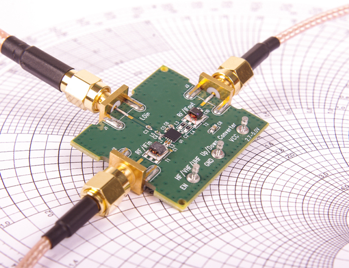
In modern wireless communication systems, IoT devices, radar modules, and microwave electronic products, RF PCB design and assembly serve as the core foundation of high-frequency circuit performance. Unlike conventional low-speed PCBs, RF (Radio Frequency) printed circuit boards operate at high frequency bands ranging from hundreds of megahertz to tens of gigahertz, where minor design flaws, layout deviations, or assembly defects can lead to severe signal attenuation, crosstalk interference, impedance mismatch, and even complete system failure. Mastering professional RF PCB design rules and standardized assembly processes is critical to ensuring low noise, high stability, and high precision of wireless electronic devices. This comprehensive guide elaborates on core design principles, key layout techniques, material selection standards, standardized assembly workflows, common defects, and optimization solutions for RF PCBs, providing actionable technical support for engineers and manufacturers engaged in high-frequency circuit development and production.
1. Core Differences Between RF PCB and Conventional PCB Design
Most electronic engineers are familiar with low-speed digital PCB design, which prioritizes wiring density, component layout aesthetics, and basic circuit connectivity. However, RF PCB design focuses entirely on high-frequency signal integrity, electromagnetic compatibility (EMC), impedance matching, and low signal loss, with fundamental differences in design logic and technical requirements.
First, conventional PCBs treat circuit traces as simple conductive wires, while RF PCB traces are essential components of the RF circuit. At high frequencies, trace width, trace length, spacing, and dielectric thickness directly affect impedance characteristics, signal phase, and transmission loss. Any unreasonable layout will change the circuit’s matching state and degrade RF performance .
Second, RF circuits are extremely sensitive to electromagnetic interference. Digital low-speed circuits can tolerate minor crosstalk and noise, but RF weak signal reception systems require strict isolation between high-power transmitting circuits and low-noise receiving circuits to avoid signal leakage and interference .
Third, RF PCB design requires strict manufacturing and assembly tolerance control. Conventional PCBs allow trace width deviations of ±0.1mm, while high-precision RF PCBs require impedance tolerance control within ±5%, putting forward higher requirements for board fabrication accuracy and assembly precision .
In summary, RF PCB design is a systematic engineering discipline integrating electromagnetic field theory, circuit theory, and manufacturing process technology, while standardized assembly is the key to converting design advantages into actual product performance.
2. Key Principles of Professional RF PCB Design
High-quality RF PCB products start with standardized design. All layout and stacking schemes must follow high-frequency electromagnetic transmission rules, with core principles covering material selection, layer stackup design, impedance control, signal isolation, and grounding optimization.
2.1 RF PCB Material Selection Standards
Substrate material performance determines the upper limit of RF PCB high-frequency performance. Low-frequency FR-4 materials are low-cost but suffer from high dielectric loss, unstable dielectric constant, and severe signal attenuation at frequencies above 1GHz, making them unsuitable for high-precision RF scenarios. For RF and microwave circuits, professional high-frequency substrates must be selected based on operating frequency and application requirements.
Common RF PCB materials include Rogers series, Taconic, and Isola high-frequency substrates. These materials feature stable dielectric constant (DK), low dielectric loss (DF), low thermal expansion coefficient, and excellent high-frequency signal transmission performance. In general, the higher the operating frequency, the lower the DF value required for the substrate to reduce high-frequency signal loss . For low-cost medium-frequency RF products (1GHz–2GHz), modified FR-4 materials can be used for cost balancing; for high-frequency microwave products (above 5GHz), Rogers 4350B, 5880, and other high-precision substrates are mandatory.
In addition, solder mask selection also affects RF performance. For key high-frequency traces, exposed copper processing is often adopted instead of conventional solder mask coverage, as solder mask materials cause minor dielectric changes that affect impedance stability .
2.2 Scientific PCB Layer Stackup Design
Layer stackup is the foundation of RF PCB signal integrity and grounding design. A reasonable stackup structure can effectively suppress crosstalk, reduce radiation noise, and ensure continuous signal return paths. The most classic and practical RF PCB stackup structure is a four-layer design, which is widely used in most wireless communication modules .
4-Layer RF PCB Standard Stackup:
Layer 1 (Top Layer): RF signal traces and key component placement area, adopting short, straight, and refined wiring to reduce parasitic parameters.
Layer 2 (Ground Plane): Complete and uninterrupted global ground plane, providing stable reference ground for top-layer RF signals and isolating upper and lower layer interference. Ground plane splitting is strictly prohibited in RF core areas .
Layer 3 (Power Plane): Independent power distribution layer, completing power supply routing for chips and components, with local ground filling for auxiliary shielding.
Layer 4 (Bottom Layer): Auxiliary wiring, test points, and non-critical low-speed signal circuits.
For high-precision multi-layer RF boards (6-layer and above), the core principle remains unchanged: separate RF signal layers, ground layers, and power layers at intervals, maximize the area of complete ground planes, and avoid overlapping RF signals with digital signal layers to eliminate cross-layer coupling interference.
2.3 Precise Impedance Control Design
Impedance matching is the core of RF PCB design. The fundamental goal is to ensure consistent characteristic impedance of signal transmission paths, eliminate signal reflection and standing wave effects, and maximize RF signal transmission efficiency. Most RF communication systems adopt 50Ω standard impedance matching, while differential RF circuits use 100Ω impedance design .
RF PCB impedance is affected by four core factors: substrate dielectric constant, dielectric thickness between signal layer and ground layer, trace width, and trace copper thickness. In the design stage, engineers must use professional impedance calculation tools to simulate and calibrate parameters, and formulate strict tolerance standards (controlled within ±5% for high-precision RF products) .
In actual layout, sudden changes in trace width are strictly prohibited. All RF high-frequency traces must maintain uniform width and avoid bending and branching at will. For impedance matching networks (L-type, π-type, T-type), passive components must be placed tightly close to the chip pin or antenna port, with ultra-short connecting traces to avoid parasitic impedance interference . In addition, production test coupons need to be reserved on the PCB for subsequent impedance testing and verification to ensure consistency between design and actual production parameters.
2.4 Signal Isolation and Anti-Interference Design
RF circuits face two major interference sources: internal digital circuit switching noise and external electromagnetic radiation interference. Effective signal isolation design is required to ensure stable operation of weak RF signals.
First, implement functional zoning layout. Strictly partition the PCB area into RF transmitting area, RF receiving area, digital logic area, and power supply area. Physically separate high-power transmitting circuits and high-sensitivity receiving circuits to prevent transmit signal leakage from interfering with weak signal reception .
Second, standardize trace spacing and crossing rules. Parallel RF traces must maintain a spacing of more than 3 times the trace width to reduce crosstalk coupling. RF signals and digital signals are prohibited from parallel wiring for long distances; if crossing is unavoidable, adopt 90° vertical crossing to minimize electromagnetic coupling area .
Third, optimize via design. Vias are a major source of high-frequency signal loss and interference. In RF design, minimize the number of signal vias to avoid destroying the integrity of the ground plane. For necessary vias, use back-drilling or blind buried via processes to eliminate via stub effects and reduce resonant interference caused by residual stubs . At the same time, arrange shielding via fences around RF core circuits and perform via stitching at intervals to form a closed shielding structure and suppress signal radiation .
2.5 Grounding Optimization Design
Good grounding is the simplest and most effective EMC solution for RF PCBs. The core grounding principle is continuous, complete, and low impedance. Many RF performance failures are caused by incomplete ground planes and discontinuous signal return paths .
RF core areas must use a complete ground plane without any splitting or slotting, as ground gaps will cause signal return path deviation, generate parasitic inductance, and lead to signal attenuation and crosstalk. All component grounding pads adopt multi-point grounding to reduce grounding impedance. For high-frequency chips and power amplifier components, add intensive grounding vias to connect the top ground and inner main ground plane to form a three-dimensional low-impedance grounding system .
In addition, separate analog ground and digital ground in complex systems, and perform single-point grounding integration at key positions to avoid digital noise conduction to the RF analog circuit through the ground loop, ensuring the purity of RF weak signals.
3. Standardized RF PCB Assembly Process
Excellent design schemes must rely on standardized RF PCB assembly processes to achieve ideal performance. RF PCB assembly has stricter process requirements than conventional PCB assembly, especially in component placement accuracy, soldering process, thermal management, and post-assembly debugging. Minor assembly deviations will offset design optimization effects and cause RF performance degradation.
3.1 Pre-Assembly Preparation and DFM Verification
Before formal assembly, complete DFM (Design for Manufacturability) and DFR (Design for Reliability) verification is required to check whether the design file matches the assembly process capability . Professional engineers need to verify key parameters such as component pad size, trace spacing, via aperture, and impedance tolerance to eliminate process risks such as difficult soldering, short circuit, and open circuit caused by design mismatch.
At the same time, strictly inspect incoming materials, including RF high-precision chips, inductors, capacitors, antennas, and PCB substrates. Check component precision grades, material consistency, and PCB surface flatness to ensure all materials meet high-frequency assembly standards. For RF passive components with high precision requirements, screen and batch test to eliminate defective parts with parameter deviation.
3.2 SMT Placement Process for RF Components
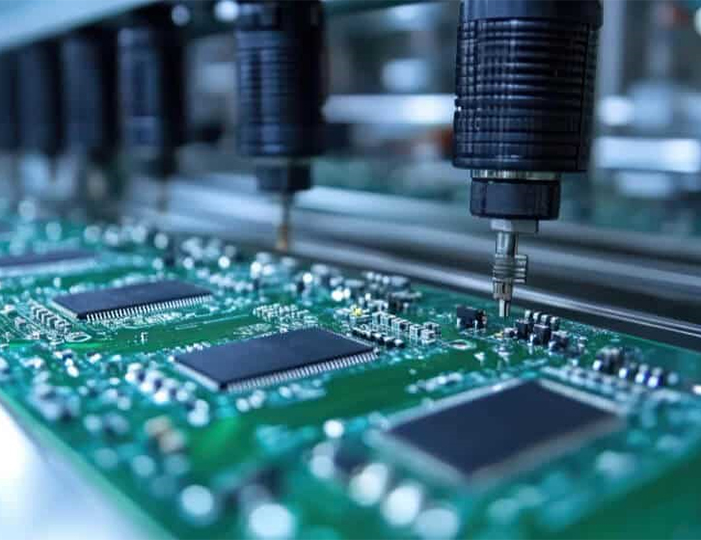
RF PCB assembly mainly adopts SMT surface mount technology. Compared with through-hole mounting, SMT has shorter signal paths, smaller parasitic parameters, and higher assembly precision, which is more suitable for high-frequency RF circuit production .
Component placement accuracy is the key to RF assembly. RF matching components, antenna pins, and transceiver chip pins require placement accuracy within ±0.02mm to avoid impedance mismatch caused by offset placement. During placement, follow the zoning design principle: place high-power devices in concentrated areas, keep weak signal devices away from heat sources and interference sources, and ensure compact and orderly placement of matching network components with no offset or rotation .
In addition, strictly control the placement direction of RF differential components and symmetric components to avoid performance deviation caused by inconsistent device orientation, ensuring consistent circuit symmetry and stable impedance matching.
3.3 Precision Soldering and Thermal Management
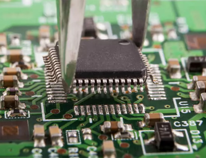
High-frequency RF components are sensitive to temperature, and excessive soldering temperature or long high-temperature time will cause component parameter drift, substrate deformation, and even device damage. Therefore, RF PCB soldering must adopt a precise temperature control reflow soldering process, formulate segmented temperature curves according to component characteristics and substrate materials, and avoid thermal shock .
For high-power RF power amplifier modules and heat-generating components, design thermal vias and copper foil heat dissipation structures in advance during the design stage. During assembly, ensure full contact between component pads and PCB solder joints to reduce thermal resistance and avoid performance degradation caused by component overheating during operation.
Strictly control solder paste thickness and soldering quality to prevent common defects such as virtual soldering, missing soldering, tin bridging, and solder ball residue. Solder ball debris on RF traces will cause signal short circuit and high-frequency resonance, seriously affecting RF signal transmission performance .
3.4 Post-Assembly Cleaning and Shielding Installation
Flux residue after soldering is a hidden danger for RF circuit failure. Residual flux will form a dielectric layer on the PCB surface, change local impedance characteristics, and absorb moisture to cause leakage and interference. Therefore, all assembled RF PCBs must undergo professional ultrasonic cleaning and ion cleaning to completely remove flux, tin residue, and dust impurities .
After cleaning and drying, install shielding cans for RF core circuits as required. Metal shielding cans can effectively isolate external electromagnetic interference and prevent internal high-frequency signal radiation leakage. During installation, ensure close contact between the shielding can and the PCB ground pad to form a complete grounding shielding system and achieve optimal isolation effect.
3.5 Post-Production Testing and Performance Verification
Different from conventional PCB functional testing, RF PCB finished product testing focuses on high-frequency performance parameter verification, including S-parameter testing, impedance testing, signal insertion loss, return loss, crosstalk interference, and electromagnetic radiation performance testing .
Use professional vector network analyzers to test key indicators of RF circuits, verify whether impedance matching, signal loss, and isolation meet design standards, and screen out defective products with performance deviation. At the same time, conduct aging tests and high and low temperature environmental tests to verify the stability and reliability of RF PCBs in complex working environments, ensuring long-term stable operation of products .

4. Common RF PCB Design & Assembly Defects and Optimization Solutions
In actual project development and mass production, engineers often encounter RF performance problems caused by design or assembly defects. Summarizing common faults and targeted optimization strategies can effectively improve product yield and performance stability.
4.1 Signal High Loss and Low Sensitivity
Causes: Unreasonable stackup design, discontinuous ground plane, excessive via stubs, long and irregular RF traces, and unqualified substrate dielectric loss. Assembly problems include offset placement of matching components and virtual soldering leading to increased circuit resistance.
Optimization Solutions: Adopt standard layered stackup, keep RF ground plane complete, use back-drilling process to eliminate via stubs, shorten RF signal traces as much as possible, and select low-DF high-frequency substrates. Strictly control component placement accuracy and soldering quality during assembly to ensure reliable circuit conduction .
4.2 Severe Signal Crosstalk and EMI Interference
Causes: Too small spacing between parallel traces, mixed layout of digital and RF signals, incomplete shielding via fences, and poor grounding leading to ground loop noise.
Optimization Solutions: Increase RF trace spacing, separate digital and RF circuit zoning completely, add dense shielding via stitching around core circuits, optimize grounding design to eliminate ground gaps, and install high-precision shielding cans for isolation .
4.3 Impedance Mismatch and Standing Wave Abnormity
Causes: Inaccurate impedance simulation in design stage, inconsistent trace width, unreasonable matching component parameters, and PCB manufacturing tolerance deviation exceeding the standard.
Optimization Solutions: Re-calibrate impedance parameters with professional simulation tools, standardize trace routing specifications, optimize matching network layout, and cooperate with manufacturers to strictly control production tolerances. Verify impedance through test coupons to ensure consistency between design and actual products .
4.4 Poor Product Consistency in Mass Production
Causes: Unstable assembly process parameters, inconsistent solder paste printing thickness, and inconsistent component placement accuracy in batch production.
Optimization Solutions: Form standardized assembly process documents, fix reflow soldering temperature curves and placement process parameters, conduct batch sampling testing of impedance and RF performance, and adjust process parameters in real time to ensure consistent batch product performance .
5. Industry Application Scenarios of High-Performance RF PCB
With the rapid development of wireless communication technology, RF PCB design and assembly technology has been widely used in high-precision electronic fields, and different scenarios have differentiated technical requirements for RF PCB performance.
5G Communication Modules: 5G high-frequency millimeter-wave products require ultra-low loss RF PCBs, high-precision impedance control, and strict EMI shielding design, supporting high-speed signal transmission and low-delay communication.
IoT Wireless Devices: Low-power Bluetooth, WiFi, and ZigBee modules require miniaturized RF PCB layout, compact assembly, and low power consumption design, balancing performance and product volume.
Radar and Microwave Devices: Automotive radar, industrial detection radar, and microwave sensing equipment require high-stability RF substrates and high-precision assembly processes, adapting to high-frequency and high-sensitivity detection scenarios.
Aerospace and Military Electronic Equipment: Strict requirements for environmental adaptability and reliability, needing high-temperature resistant, anti-interference, and high-stability RF PCB design and standardized high-reliability assembly processes.
RF PCB design and assembly is a high-precision technical work integrating electromagnetic simulation, structural design, material science, and precision manufacturing. Excellent RF performance depends on standardized design rules in the early stage and rigorous assembly processes in the later stage. In the design process, it is necessary to focus on material selection, layer stackup, impedance control, signal isolation, and grounding optimization to eliminate inherent performance risks; in the assembly process, strictly implement DFM verification, precision placement, temperature-controlled soldering, and professional testing to ensure that the design effect is perfectly presented.
With the continuous upgrading of wireless communication technology, the operating frequency of electronic products continues to improve, and the performance requirements for RF PCBs will become more stringent. Only by mastering systematic design methods and standardized assembly processes, continuously optimizing technical details, and avoiding common defects can we produce high-stability, low-loss, and high-reliability RF PCB products to meet the technical needs of 5G, IoT, radar, and other high-end fields.
Lucy Yang | lucy.y@toxutech.com
Dotty Zhao | sales04@toxutech.com
Global Business Director / Sales Team / Global Operations


 En
 Cn
 Korean
 Home >
