

-
Products -PCBA Manufacturing RF Connectors RF Cable Assemblys Embedded Antennas External Antennas GNSS Positioning Solutions
RF Connectors

RF Cable Assemblys
Embedded Antennas
External Antennas
GNSS Positioning Solutions



 Language


Language


Time:2026-10-17 Views:0
The transition from RF device prototype to mass production is one of the most critical and complex phases in wireless communication hardware development. Radio Frequency (RF) devices serve as the core backbone of modern wireless systems, including 5G/6G base stations, IoT sensors, Bluetooth modules, Wi-Fi transceivers, satellite communication equipment, and industrial radio devices. While prototyping focuses on functional verification and theoretical performance validation, mass production demands consistent quality, high yield rates, cost control, strict compliance with industry standards, and scalable manufacturing processes. Many RF hardware projects fail to launch commercially not due to flawed prototype design, but due to unoptimized transition workflows, unaddressed manufacturing limitations, and overlooked RF-specific performance degradation risks during scaling. This comprehensive guide explores the end-to-end process of moving RF device prototypes to mass production, breaks down core challenges, shares industry-proven best practices, and highlights key optimization strategies to help hardware developers, manufacturing engineers, and product teams achieve reliable, high-volume, and cost-effective RF device manufacturing.
1. Core Differences: RF Prototype vs. Mass-Produced RF Device
Before initiating the transition from RF prototype to mass production, it is essential to clarify the fundamental differences between prototype-stage development and commercial mass production. Unlike general electronic devices, RF products are extremely sensitive to material consistency, process precision, environmental interference, and assembly tolerance. A prototype that performs perfectly in a laboratory environment often faces severe performance attenuation, signal distortion, and stability issues after mass manufacturing. The key differences are summarized below to clarify transition priorities.
1.1 Design Purpose & Evaluation Standards
RF device prototypes are designed for functional verification and performance proof-of-concept. The primary goal is to confirm that the circuit design, RF signal transmission, frequency response, impedance matching, and power consumption meet theoretical design indicators. Laboratory prototype testing focuses on ideal environmental conditions—stable temperature, no electromagnetic interference (EMI), precise manual debugging, and selected high-precision components. Evaluation standards prioritize technical indicators such as gain, return loss, insertion loss, frequency bandwidth, and signal-to-noise ratio (SNR), with almost no consideration of production cost, batch consistency, or long-term reliability.
In contrast, mass-produced RF devices target commercial applicability, batch stability, and market compliance. Evaluation standards cover not only core RF performance but also production yield, unit cost, environmental adaptability, service life, EMI/EMC compliance, and batch consistency. Every production link must be standardized to ensure that tens of thousands or millions of products maintain consistent RF performance under complex industrial and outdoor working conditions.
1.2 Component Selection & Material Requirements
Prototype-stage RF devices usually adopt high-precision, high-cost laboratory-grade components, including military-grade RF resistors, capacitors, inductors, and customized RF chips. Developers prioritize performance over cost and availability, and component parameter tolerances are extremely strict (±0.1% or lower). In addition, prototype PCB substrates often use high-end imported microwave substrates with excellent dielectric constant stability, which are costly and have long delivery cycles, making them unsuitable for large-scale procurement.
For mass production, component selection must balanceperformance, cost, supply stability, and process compatibility. Engineers need to replace non-mass-producible prototype components with industrial-grade standardized parts, verify parameter tolerance adaptability (usually ±1%~±5% tolerance), and establish dual or multiple supplier supply chains to avoid production shutdown risks caused by single-source component shortages. Meanwhile, PCB substrate materials need to be upgraded to mass-production-grade microwave substrates with stable dielectric constants, low loss tangent, and cost advantages, ensuring consistent RF signal transmission performance in batch production.
1.3 Manufacturing Process & Assembly Mode
RF prototypes are mostly assembled manually by senior RF engineers, with precise manual debugging of impedance matching networks, antenna parameters, and circuit bias points. Manual assembly allows fine-tuning for individual device defects, compensating for design or component tolerances. However, manual operation is highly dependent on personal experience, with low efficiency and no unified process standards, making it impossible to replicate in mass production.
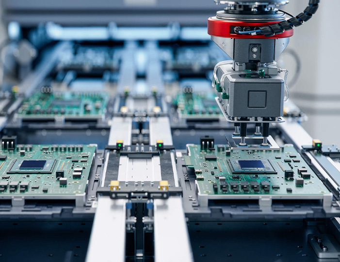
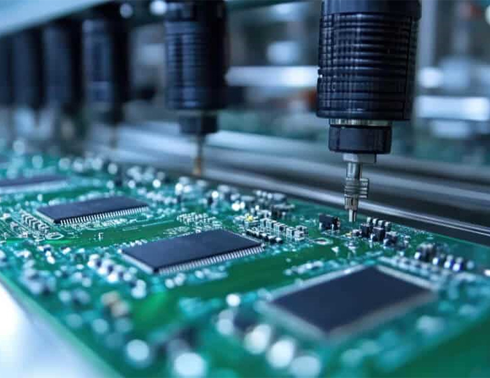
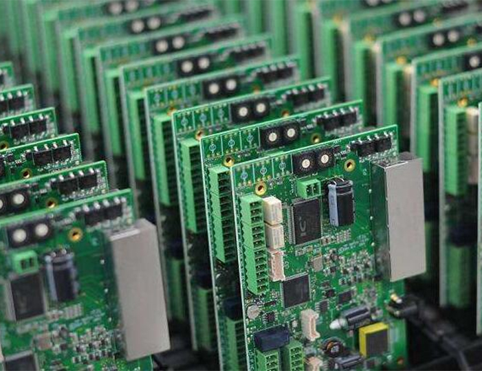
Mass production relies entirely on automated SMT assembly, standardized reflow soldering, robotic welding, and automated calibration processes. All assembly parameters, soldering temperatures, feeding speeds, and calibration procedures must be solidified into standardized production instructions. The process design must eliminate manual debugging links and ensure that all RF performance indicators can be stably replicated through automated equipment, achieving batch consistency of products.
2. End-to-End Workflow for RF Device Prototype to Mass Production Transition
The transition from RF prototype to mass production is a systematic project covering design optimization, process verification, sample iteration, pilot production, and formal volume production. The entire workflow can be divided into six core stages, each with clear verification indicators and deliverables, which is the key to ensuring a smooth and low-risk transition.
2.1 Stage 1: Prototype Design Review & Manufacturability Optimization (DFM for RF)
Design for Manufacturability (DFM) is the first and most critical step in the transition process. Most laboratory RF prototypes have design defects that are not suitable for mass production, including unreasonable circuit layout, insufficient process tolerance margins, unoptimized impedance matching structures, and over-reliance on manual debugging. RF DFM optimization is different from conventional electronic DFM; it must fully consider the unique characteristics of RF signal transmission.
First, complete RF circuit layout optimization. High-frequency RF signals are extremely sensitive to trace width, trace spacing, via size, and grounding design. Prototype layouts often pursue ideal electrical performance, ignoring the tolerance errors of automated SMT production. In mass production optimization, engineers need to widen the process tolerance window of key RF traces, standardize via distribution to avoid signal leakage and crosstalk, and optimize the grounding network to reduce ground impedance fluctuation in batch production. For high-frequency RF circuits above 1GHz, it is necessary to simulate the impedance deviation caused by batch PCB manufacturing errors and reserve sufficient design margin.
Second, simplify over-optimized prototype designs. Many prototype designs adopt redundant circuit structures and high-precision components that exceed commercial product requirements, leading to excessive production costs. The DFM team needs to delete redundant functional circuits, replace over-spec components with industrial-grade alternative parts, and verify that the simplified design can still meet all commercial performance indicators. This step can effectively reduce the BOM cost of RF devices by 15%–35%.
Third, complete BOM standardization and supply chain sorting. Sort out all prototype components, eliminate discontinued parts, long-delivery customized parts, and single-source high-risk parts, and complete component alternative verification. Establish a standardized mass-production BOM, mark key components and alternative models, and confirm batch procurement prices and delivery cycles with suppliers to ensure supply stability for long-term mass production.
2.2 Stage 2: RF Performance Simulation & Tolerance Analysis
After DFM optimization, targeted RF performance simulation and batch tolerance analysis must be carried out to predict performance fluctuations in mass production. Conventional prototype testing only verifies the performance of a single sample, while mass production faces superposition errors of PCB manufacturing tolerance, component parameter tolerance, assembly process tolerance, and environmental temperature drift.
Engineers need to use professional RF simulation software (ADS, HFSS, CST) to conduct Monte Carlo tolerance simulation, covering key indicators such as return loss, insertion loss, gain flatness, phase noise, and harmonic suppression. By simulating the performance changes of RF devices under different parameter tolerance combinations, screen out sensitive design links with small tolerance margins, and carry out secondary optimization for vulnerable points. For example, for the impedance matching network most sensitive to component tolerance, optimize the circuit structure to reduce the sensitivity of RF performance to resistance and capacitance deviation, ensuring that 99.9% of batch products can meet the performance standard.
In addition, complete environmental adaptability simulation, including high and low temperature cycle, humidity aging, and vibration shock simulation. Verify the stability of RF performance under extreme working conditions, avoid mass performance failure caused by environmental changes after product launch, and improve the long-term reliability of mass-produced products.
2.3 Stage 3: Engineering Sample Iteration & Reliability Testing
After design optimization and simulation verification, engineering sample (EVT/DVT) iteration is carried out, which is the bridge connecting prototypes and mass production. Different from laboratory prototypes, engineering samples are produced according to preliminary mass production processes and standardized components, which can truly reflect the performance level of mass-produced products.
The EVT (Engineering Verification Test) stage focuses on verifying the feasibility of the optimized design and preliminary process parameters. Produce 50–200 engineering samples, conduct full-item RF performance testing, functional testing, and structural matching testing. Screen out design defects, process mismatches, and performance inconsistency problems, and complete design revision and process adjustment.
The DVT (Design Verification Test) stage is oriented to mass production reliability. On the basis of finalized EVT design, produce 200–500 samples with formal mass production materials and process parameters, and complete full-standard reliability testing, including EMI/EMC electromagnetic compatibility testing, high and low temperature aging testing, power-on long-term operation testing, mechanical vibration testing, and waterproof and dustproof testing according to IP standards. All test results must meet industry certification standards (CE, FCC, RoHS) and customer technical specifications, and form a complete reliability test report.
2.4 Stage 4: Process Solidification & Production Line Validation (PVT)
Production Verification Test (PVT) is the core stage of transforming design capability into mass production capability. The core goal is to solidify all production processes, equipment parameters, and operation specifications to ensure batch consistency and high yield rate of RF devices.
First, solidify standardized production processes, including SMT stencil design, solder paste printing parameters, reflow soldering temperature curve, component mounting accuracy standards, RF calibration procedures, and finished product testing processes. For RF devices, the calibration process is particularly critical; manual calibration in the prototype stage must be replaced by automated RF testing and calibration equipment to eliminate human error. Solidify the test threshold of each RF indicator to ensure unified judgment standards for qualified products.
Second, complete production line debugging and capacity verification. Arrange special production line equipment for RF products, calibrate the precision of SMT mounting equipment, RF comprehensive tester, network analyzer, and signal generator to ensure test accuracy and consistency. Carry out small-batch trial production of 1000–3000 units, count the production yield rate, count defective product types and failure rates, and formulate targeted process improvement plans for defective links such as poor soldering, offset mounting, and unqualified RF performance.
Finally, form complete mass production documents, including BOM list, PCB manufacturing specifications, production operation instructions (SOP), test specifications, quality inspection standards, and after-sales maintenance specifications. All documents are unified and filed to provide standardized guidance for formal mass production.
2.5 Stage 5: Pilot Mass Production & Yield Rate Optimization
Pilot mass production is the final risk assessment before large-scale volume production, aiming to verify the stability of the production system, supply chain matching degree, and batch product consistency. The pilot production batch is usually 5000–10000 units, and the entire production process is fully simulated according to formal mass production modes, including material incoming inspection, production line assembly, automated testing, quality screening, packaging and warehousing.
During pilot production, focus on monitoring three core indicators: product yield rate, batch performance consistency, and production efficiency. Count the primary yield rate and secondary repair yield rate of each production link, analyze the root cause of unqualified products (design tolerance, process error, material defect, or test error), and complete closed-loop optimization. For RF devices with complex structures, the primary yield rate of pilot production is usually 85%–90%, and continuous process optimization is required to raise the mass production yield rate to more than 95% to meet commercial profit requirements.
At the same time, verify the supply chain stability during pilot production, evaluate the delivery speed and quality consistency of bulk materials, adjust the material procurement cycle and inventory strategy, and avoid production stagnation caused by material shortages or batch material quality problems.
2.6 Stage 6: Formal Mass Production & Continuous Quality Control
After the pilot production yield rate, product performance, and process stability meet the standards, formal large-scale mass production can be launched. In the formal production stage, the core work is to maintain process stability, realize continuous quality control, and optimize production costs.
Establish a full-process quality monitoring system: carry out sampling inspection for each batch of incoming materials, conduct real-time monitoring of production line process parameters, spot-check RF performance of finished products in batches, and track product operation data after delivery. For key RF indicators with large fluctuation risks, set up early warning mechanisms to quickly respond to abnormal batch quality.
Carry out continuous cost optimization: on the premise of ensuring product performance and quality, further optimize the BOM structure, reduce redundant processes, improve production line automation efficiency, and reduce unit production and labor costs. At the same time, establish a regular process review mechanism, continuously optimize production details according to mass production data, and improve product yield and production capacity.
3. Key Challenges in RF Device Prototype to Mass Production Transition
Compared with conventional electronic products, RF device scaling has unique technical and process challenges, which are the main reasons for low yield rate and project delay in the transition process. Mastering these core challenges and targeted solutions is the key to successful mass production.
3.1 RF Performance Batch Consistency Problem
High-frequency RF signals are extremely sensitive to tiny changes in production processes. PCB substrate dielectric constant deviation, trace width tolerance, component parameter drift, and soldering tin thickness difference will all lead to fluctuations in impedance matching, resulting in inconsistent key indicators such as product gain, return loss, and frequency response. A single prototype can achieve optimal performance through precise debugging, but batch products are prone to individual performance differences, which seriously affects product qualification rate and market applicability.
Solutions: Optimize design tolerance margin through Monte Carlo simulation, select high-stability materials and components with low temperature drift, solidify automated precision assembly and calibration processes, and eliminate manual debugging errors. Establish batch performance big data monitoring to dynamically adjust process parameters and ensure batch consistency.
3.2 EMI/EMC Compliance Risks in Mass Production
Laboratory prototypes usually have simple structural shielding and no standardized EMI processing, and can pass short-term laboratory tests. However, in mass production, due to inconsistent shielding assembly, grounding process deviation, and component batch differences, products are prone to electromagnetic interference and electromagnetic radiation exceeding standards, failing to meet FCC, CE and other certification requirements, resulting in product sales restrictions.
Solutions: Complete standardized EMI shielding design in the DFM stage, solidify shielding cover assembly and grounding process specifications, increase batch EMI sampling test links in mass production, and optimize circuit anti-interference design for high-risk interference points.
3.3 Low Production Yield Rate Caused by Process Tolerance
Many RF prototype designs have insufficient process tolerance margins, which can adapt to high-precision manual production but cannot adapt to the tolerance errors of automated mass production. Tiny deviations in SMT mounting position, soldering temperature, and via processing will lead to RF performance failure, resulting in low primary yield rate, increased repair costs, and reduced production efficiency.
Solutions: Carry out full-process process tolerance analysis before mass production, optimize vulnerable design links, adjust production equipment precision parameters, formulate strict process operation standards, and conduct regular equipment calibration and process audits.
3.4 Supply Chain Instability of Special RF Components
High-performance RF chips, microwave substrates, and high-precision passive components are mostly monopolized by overseas manufacturers, with long delivery cycles, price fluctuations, and shortage risks. Prototype-stage small-batch procurement can meet demand, but large-scale mass production is easily affected by supply chain fluctuations, leading to production shutdowns and delivery delays.
Solutions: Establish dual-supplier and multi-region supply mechanisms, complete alternative component verification in advance, reserve bulk material inventory for key components, and sign long-term supply cooperation agreements with suppliers to stabilize supply and price.
4. Industry-Proven Best Practices for RF Mass Production Transition
Based on the mass production experience of 5G RF modules, IoT RF transceivers, and industrial RF communication devices in the industry, the following best practices can effectively reduce transition risks, shorten the project cycle, and improve product yield and market competitiveness.
4.1 Advance RF-Specific DFM Optimization
Take RF performance stability as the core of DFM optimization, rather than only focusing on conventional structural and assembly manufacturability. Prioritize optimizing high-frequency signal lines, impedance matching networks, grounding systems, and shielding structures, reduce the sensitivity of RF performance to process errors, and reserve sufficient tolerance margins for batch production. Avoid over-design and over-precision configuration of prototypes to balance performance and cost.
4.2 Build a Full-Stage Test Verification System
Establish a layered test system covering prototype verification, engineering sample testing, pilot production testing, and formal mass production testing. Equip professional RF testing equipment such as network analyzers, signal analyzers, and comprehensive RF testers to realize automated, high-precision, and standardized testing. Form exclusive test standards for different RF indicators to ensure that all performance deviations can be accurately identified and corrected.
4.3 Solidify Automated Calibration & Production Processes
Completely abandon the manual debugging mode of prototypes, realize full-process automated assembly, testing, and calibration. Develop exclusive automated calibration software and process programs for RF devices, unify the calibration parameters of batch products, eliminate human-induced performance differences, and greatly improve production efficiency and batch consistency.
4.4 Realize Closed-Loop Management of Production Data
Access mass production test data and production process data to realize real-time monitoring and big data analysis of product performance. Track the performance changes of each batch of products, summarize the correlation between process parameters and RF performance, continuously optimize production processes and design schemes, and form a closed-loop iteration mechanism of "design-production-test-optimization".
4.5 Strictly Control Material Batch Consistency
RF device performance is highly dependent on material consistency. Establish strict incoming material inspection standards, conduct special performance testing for key RF materials and components, and reject batches with inconsistent parameters. For core materials such as microwave substrates and RF chips, fix supplier models and production batches to avoid performance fluctuations caused by material replacement.
5. Common Mistakes to Avoid in RF Prototype Mass Production Transition
In actual project operation, many teams fall into typical transition mistakes, leading to prolonged project cycles, increased costs, and unqualified mass production products. The following common mistakes need to be strictly avoided:
First, directly mass-producing based on prototype design without DFM optimization. Laboratory prototypes are not designed for mass production, and direct scaling will lead to a large number of batch performance defects and low yield rate.
Second, ignoring tolerance simulation and batch performance verification. Only testing single prototype performance without considering batch superposition errors will lead to mass performance failure after production launch.
Third, retaining manual debugging links in mass production. Manual operation cannot be replicated in batch production, which will lead to uncontrollable product consistency and inability to form standardized production.
Fourth, neglecting supply chain risk management. Relying on a single supplier for key RF components will lead to production interruption risks, affecting product delivery and market layout.
Fifth, incomplete reliability testing. Insufficient environmental aging and EMI testing in the sample stage will lead to frequent product failures after market launch, increasing after-sales costs and damaging brand reputation.
The transition from RF device prototype to mass production is a systematic engineering process that integrates design optimization, process innovation, quality control, and supply chain management. Its core essence is to transform the ideal laboratory performance of RF prototypes into stable, consistent, low-cost, and commercially viable mass production capabilities. Different from ordinary electronic product scaling, RF device transition needs to focus on signal stability, batch consistency, and process tolerance adaptability, solve unique problems such as RF performance fluctuation and EMI compliance risks, and rely on standardized design optimization, automated production processes, and full-link quality monitoring to achieve seamless transition.
For wireless hardware enterprises and R&D teams, mastering the scientific prototype-to-mass-production transition workflow and best practices can effectively shorten the product launch cycle, reduce R&D and production costs, improve product yield and market competitiveness, and lay a solid foundation for the large-scale commercial application of 5G/6G communication, IoT, satellite communication, and industrial wireless RF devices. With the continuous upgrading of wireless communication technology, the precision and performance requirements of RF devices will continue to improve, and standardized, automated, and intelligent mass production transition will become the core competitiveness of RF hardware enterprises in the industry.
Lucy Yang | lucy.y@toxutech.com
Dotty Zhao | sales04@toxutech.com
Global Business Director / Sales Team / Global Operations


 En
 Cn
 Korean
 Home >
