

-
Products -PCBA Manufacturing RF Connectors RF Cable Assemblys Embedded Antennas External Antennas GNSS Positioning Solutions
RF Connectors

RF Cable Assemblys
Embedded Antennas
External Antennas
GNSS Positioning Solutions

 Language


Language


Time:2026-10-21 Views:0
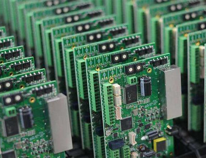
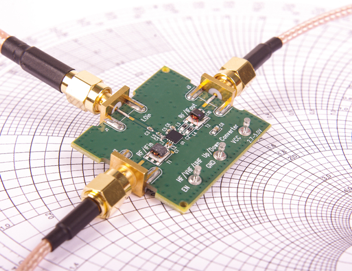
High frequency RF PCB assembly is a specialized electronic manufacturing service dedicated to the fabrication and assembly of radio frequency and microwave printed circuit boards operating at frequencies typically above 300 MHz, extending to millimeter-wave bands for 5G, 6G, radar, and satellite communication systems. Unlike conventional low-frequency PCB assembly, high-frequency RF PCB assembly demands ultra-precise process control, strict impedance stability, minimal signal loss, and zero interference contamination, as high-frequency electromagnetic signals are extremely sensitive to material changes, assembly tolerances, and residual impurities. As wireless communication, aerospace defense, IoT smart sensing, and automotive radar industries rapidly evolve, professional high frequency RF PCB assembly has become a core manufacturing link that determines the performance, stability, and service life of high-end RF electronic equipment.
In commercial electronic manufacturing, standard PCBs are usually suitable for DC to low-frequency AC signal transmission, where minor assembly deviations or material defects barely affect overall circuit performance. However, RF and microwave circuits rely on high-frequency electromagnetic wave propagation, and subtle changes in trace width, dielectric thickness, solder residue, component placement offset, and grounding continuity will lead to signal attenuation, impedance mismatch, phase shift, noise interference, and even complete circuit failure. Therefore, high frequency RF PCB assembly is not a simple upgrade of ordinary SMT assembly but a systematic precision manufacturing technology integrating material science, radio frequency electromagnetics, precision machinery processing, and strict quality inspection. This article comprehensively elaborates on the core processes, key technical requirements, common challenges, industry best practices, typical applications, and quality control standards of high-frequency RF PCB assembly, providing authoritative guidance for engineers, procurement personnel, and electronic manufacturing enterprises.
1. Core Differences Between High Frequency RF PCB Assembly and Standard PCB Assembly
To understand the uniqueness of high frequency RF PCB assembly, it is essential to distinguish it from traditional low-frequency PCB assembly, as the core technical indicators, process standards, and manufacturing thresholds of the two are vastly different. Most low-frequency electronic products such as consumer electronics, household appliances, and ordinary industrial control boards prioritize electrical connectivity and basic stability, with low requirements for signal transmission accuracy and electromagnetic consistency. In contrast, RF high-frequency circuits take signal integrity, impedance control accuracy, and low dielectric loss as the primary manufacturing goals, putting forward extremely stringent requirements for every assembly procedure.
First, material adaptability is fundamentally different. High frequency RF PCB assembly mainly targets high-frequency special substrates including Rogers, Teflon (PTFE), FR-4 high-frequency modified materials, and ceramic substrates. These materials feature low dielectric constant (Dk), low dielectric loss (Df), stable temperature characteristics, and low electromagnetic signal attenuation, which are essential for high-speed RF signal transmission. Ordinary FR-4 substrates used in standard assembly have high dielectric loss at high frequencies, severe signal attenuation, and poor temperature stability, making them unable to meet RF circuit requirements. In addition, high-frequency substrates usually have low Tg values, being sensitive to high-temperature impact, so the reflow soldering temperature curve and thermal cycle parameters of high frequency RF PCB assembly must be specially optimized to avoid substrate warping, delamination, and performance degradation.
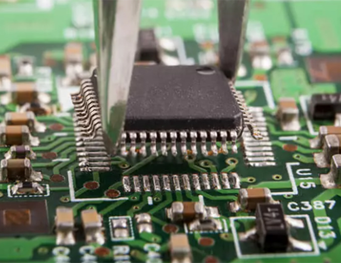
Second, assembly precision tolerance standards are completely different. Standard SMT assembly allows placement offset errors within ±0.1mm for conventional components, while high-frequency RF components such as RF connectors, microwave filters, power amplifier chips, and antenna matching components require placement coplanarity and position accuracy within ±0.05mm. Tiny placement deviations will change the geometric parameters of RF transmission lines, resulting in sudden impedance changes, signal reflection, and increased insertion loss. Moreover, high frequency RF PCB assembly prohibits irregular solder joint shapes and excessive solder volume; redundant solder will form parasitic capacitance and inductance, disrupting the matching state of RF circuits and reducing overall equipment communication efficiency.
Third, post-assembly cleaning and environmental control standards are upgraded comprehensively. Ordinary PCB assembly only requires basic flux residue cleaning to avoid short circuits and corrosion. However, high-frequency RF circuits are extremely sensitive to ionic contaminants and residual flux. Micro-scale flux residues on the surface of RF microstrip lines will form tiny conductive channels, changing the surface impedance and dielectric properties of the circuit board, leading to signal distortion and frequency drift. Therefore, high frequency RF PCB assembly must adopt professional cleaning processes such as plasma cleaning and steam degreasing instead of conventional water cleaning, which can effectively avoid moisture absorption of PTFE and Rogers substrates and eliminate micro-residues that affect high-frequency signal transmission.
Finally, quality inspection and testing standards are different. Standard PCB assembly mainly detects solder joint quality, open/short circuits, and component welding integrity through AOI and ICT tests. High frequency RF PCB assembly requires additional professional RF performance tests, including impedance testing, insertion loss, return loss, standing wave ratio (VSWR), and noise figure testing, to verify whether the circuit meets high-frequency signal transmission standards. Only when both appearance welding quality and RF electrical performance reach the standard can the assembly be deemed qualified.
2. Complete Process Flow of High Frequency RF PCB Assembly
High frequency RF PCB assembly follows a standardized and rigorous full-process manufacturing system, covering pre-production preparation, substrate pretreatment, SMT precision assembly, special soldering treatment, professional cleaning, multi-dimensional testing, and finished product packaging. Each link has customized process parameters and operation specifications to ensure the consistency and reliability of high-frequency RF circuit performance.
2.1 Pre-Production Design for Manufacturing (DFM) Review
DFM review is the primary core link of high frequency RF PCB assembly and the key to reducing production risks and improving yield. Different from ordinary PCB assembly, RF high-frequency boards have strict design-manufacturing matching requirements. Professional assembly engineers need to conduct in-depth review of PCB stackup design, impedance design, trace routing, via setting, component layout, and grounding design before production.
Key review points include: whether the high-frequency signal traces are short and direct to reduce transmission loss; whether the ground plane is continuous to provide a stable signal return path; whether ordinary vias are avoided on high-frequency main signal lines to prevent parasitic inductance and capacitance; whether differential pair routing meets high-frequency anti-interference requirements; and whether the via stub length is optimized through back-drilling technology to suppress high-frequency resonance. For unqualified design details, engineers will provide optimization suggestions in advance to avoid performance defects that cannot be remedied after assembly. Early DFM intervention can effectively reduce assembly rework rate and ensure one-time molding of high-frequency RF boards.
2.2 Substrate Inspection and Pretreatment
High-frequency substrates such as Rogers and PTFE are prone to surface scratches, oxide layers, and micro-pollution during transportation and storage, which will seriously affect soldering quality and high-frequency signal performance. Therefore, substrate pretreatment is indispensable in high frequency RF PCB assembly. First, conduct full appearance and dimensional inspection to screen out warped, delaminated, and scratched unqualified boards. Then, perform surface micro-cleaning and activation treatment to remove surface oxide and dust particles, improve solder paste adhesion, and ensure the tight combination of components and substrate.
In addition, for high-frequency boards that need exposure of partial radio frequency traces, confirm the solder mask opening accuracy to avoid solder mask covering high-frequency signal lines and affecting impedance characteristics. For multilayer high-frequency PCBs, check the alignment accuracy of inner layers to ensure the consistency of dielectric thickness and avoid local impedance deviation caused by layer offset.
2.3 Precision Solder Paste Printing
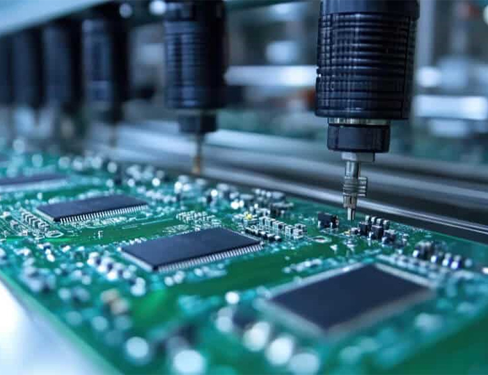
Solder paste printing directly determines the quality of RF solder joints and is a key process affecting high-frequency circuit stability. High frequency RF PCB assembly needs to select special low-residue, high-temperature-resistant RF-grade solder paste, which has stable activity, less ionic residue after welding, and will not cause long-term signal interference. The stencil thickness and opening design are customized according to RF component types: ultra-thin stencils are used for fine-pitch QFN, BGA, and RF chip components to control solder paste volume accurately and prevent solder bridging and insufficient soldering.
During printing, strictly control printing pressure, speed, and demolding speed to ensure uniform and consistent solder paste thickness without deviation, missing printing, or excessive accumulation. Uneven solder paste will lead to inconsistent solder joint sizes, form parasitic parameters, and affect the impedance matching of RF circuits. After printing, 100% solder paste thickness inspection is carried out with SPI equipment to eliminate printing defects in advance.
2.4 High-Precision Component Placement
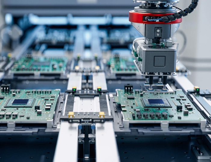
Component placement accuracy is the core of high frequency RF PCB assembly. High-frequency RF components are mostly miniaturized, high-precision devices with strict placement coplanarity and position tolerance requirements. The placement equipment needs to support micron-level precision positioning to ensure that the pin coplanarity of RF connectors, power amplifiers, filters, and antenna components meets the standard, with placement offset strictly controlled within ±0.05mm.
Special attention is paid to the placement of high-frequency signal devices: ensure that the placement direction of differential pairs is consistent, avoid angle deviation; keep the spacing of adjacent RF components uniform to prevent electromagnetic crosstalk; strictly follow the layout requirements of grounding pins to ensure full contact with the ground plane and reduce grounding impedance. For ultra-fine components such as 01005 chips, professional high-precision placement machines are used to achieve error-free mounting and avoid tiny position deviations that induce high-frequency signal attenuation.
2.5 Optimized Reflow Soldering Process
The reflow soldering process of high frequency RF PCB assembly is completely different from conventional SMT processes. High-frequency substrates represented by PTFE and Rogers have low Tg values and poor high-temperature resistance. Long-term high-temperature exposure will cause substrate warping, delamination, and changes in dielectric parameters, leading to impedance drift and signal failure. Therefore, it is necessary to customize a low-temperature, short-time high-precision reflow temperature curve.
The core optimization points include: properly reducing the peak reflow temperature, shortening the high-temperature constant time, and slowing down the heating and cooling rate to avoid thermal stress damage to high-frequency substrates. At the same time, according to the thermal characteristics of different RF components and substrates, the temperature curve is adjusted in real time to ensure full melting of solder paste, formation of smooth and full solder joints, and no thermal damage to components and substrates. Strictly avoid virtual soldering, cold soldering, and solder ball defects, which are fatal to high-frequency RF circuit performance.
2.6 Professional Post-Welding Cleaning
Post-welding cleaning is a unique key process of high frequency RF PCB assembly and an important means to eliminate high-frequency signal interference. Conventional water-based cleaning is easy to cause moisture absorption of high-frequency substrates, and residual water molecules will change the dielectric constant of the substrate, affecting signal transmission. Therefore, high-end RF assembly adopts plasma cleaning or steam degreasing processes, which can thoroughly remove micro-flux residues, ionic pollutants, and surface dust without damaging the substrate and components.
Plasma cleaning can realize microscopic activation and cleaning of circuit board surfaces, remove invisible nano-scale pollutants, effectively improve the surface insulation performance and high-frequency stability of RF boards, and ensure long-term reliable operation of high-frequency circuits in complex electromagnetic environments. For high-precision aerospace and military RF products, secondary deep cleaning and dust-free drying treatment are also required to meet ultra-high cleanliness standards.
2.7 Multi-Dimensional Quality Inspection and RF Performance Testing
The testing link of high frequency RF PCB assembly covers appearance inspection, electrical performance testing, and professional RF parameter testing, realizing full-quality control. First, AOI automatic optical inspection is used to detect solder joint defects such as virtual soldering, missing soldering, solder bridging, and offset placement to ensure assembly appearance quality. For BGA and hidden solder joints, X-ray detection is equipped to check internal soldering integrity.
On the basis of conventional electrical open/short circuit testing, professional RF performance testing is carried out, including impedance accuracy testing (tolerance controlled within ±5%), insertion loss, return loss, voltage standing wave ratio (VSWR), noise figure, and signal gain testing. These professional indicators directly determine the communication performance of RF equipment. For high-reliability products such as aerospace and automotive radar, environmental stress screening (ESS) is also required, including thermal cycling, high and low temperature aging, and vibration testing to screen out potential assembly defects and improve product stability and service life.
3. Key Technical Challenges in High Frequency RF PCB Assembly
Although the process system of high frequency RF PCB assembly is mature, it still faces many technical challenges in actual mass production and high-precision prototype manufacturing, mainly focusing on impedance stability control, anti-interference processing, substrate protection, and consistency control of mass production.
3.1 Precision Impedance Control Difficulties
Impedance matching is the core principle of high-frequency RF signal transmission, and any subtle change in the assembly process will cause impedance deviation. The impedance of RF transmission lines is affected by trace width, dielectric thickness, solder joint size, and component welding state. In the assembly process, minor deviations in solder paste printing thickness, placement position, and soldering temperature will lead to local impedance changes, resulting in signal reflection, increased return loss, and reduced transmission efficiency. Especially for millimeter-wave high-frequency circuits above 24GHz, the impedance tolerance requirement is stricter, and the assembly process window is extremely narrow, putting forward ultra-high requirements for process stability and operation precision.
3.2 Electromagnetic Crosstalk and Signal Interference Problems
High-frequency electromagnetic signals have strong radiation and coupling characteristics. In high frequency RF PCB assembly, unreasonable component spacing, irregular grounding treatment, and residual solder debris will cause electromagnetic crosstalk between adjacent signal lines and components. In addition, poor grounding continuity caused by assembly defects will lead to unstable signal return paths, generating high-frequency noise interference and seriously reducing the signal-to-noise ratio of RF circuits. For multi-channel RF transceiver boards, mutual interference between transmitting and receiving signals is more prominent, which requires precise assembly and strict electromagnetic shielding process control.
3.3 High-Frequency Substrate Thermal Damage Risk
Most high-frequency special substrates have poor thermal stability and are sensitive to thermal stress. Improper reflow temperature curve setting and excessive thermal cycles will cause substrate warping, delamination, and dielectric parameter attenuation. PTFE substrates are particularly prone to thermal deformation at high temperatures, resulting in trace offset and impedance drift, which are difficult to repair. In addition, repeated rework and welding will cause cumulative thermal damage to high-frequency boards, greatly reducing product yield and long-term reliability. Therefore, high frequency RF PCB assembly requires one-time precise molding, and rework operations are strictly limited.
3.4 Residual Pollution Induced Performance Degradation
Micro-residues generated during the assembly process are the invisible killer of high-frequency RF circuits. Flux residues, solder powder particles, and ionic contaminants will form variable dielectric layers on the surface of RF traces, changing the local Dk and Df values of the circuit board, leading to frequency drift and signal attenuation. In high-humidity environments, these residues will also absorb moisture, aggravate signal interference, and even cause micro-short circuits. Conventional cleaning processes cannot remove nano-scale residues, which is why professional plasma cleaning is a necessary process for high-end high frequency RF PCB assembly.

4. Industry Best Practices for High Frequency RF PCB Assembly
To solve the above technical challenges and ensure high performance and high reliability of assembled products, the high-frequency RF electronic manufacturing industry has summarized a set of mature best practices covering material selection, process optimization, layout matching, and quality management, which are widely used in high-end fields such as 5G communication, aerospace, and automotive electronics.
4.1 Scientific Substrate and Surface Finish Selection
Matching high-frequency substrates according to product frequency bands is the foundation of high-quality assembly. For low and medium RF frequency bands (300MHz-6GHz), modified high-frequency FR-4 and ordinary Rogers substrates can be selected to balance performance and cost; for high-frequency microwave and millimeter-wave bands (above 6GHz), high-precision Rogers and PTFE substrates with ultra-low dielectric loss are mandatory. In terms of surface finish, ENIG (electroless nickel immersion gold) and immersion silver are preferred for high frequency RF PCB assembly. These surface treatments have flat surfaces, stable chemical properties, and consistent impedance characteristics, which can avoid signal attenuation caused by uneven solder surfaces and oxidation. Ordinary tin spraying surface finish is not suitable for high-frequency RF boards due to uneven surface and easy oxidation.
4.2 Optimize Layout and Via Process to Suppress Signal Loss
Cooperate with design terminals to optimize layout and via processes in advance to reduce assembly-induced signal loss. During the DFM stage, minimize the number of vias on high-frequency main signal lines; if vias are unavoidable, adopt blind buried vias and back-drilling processes to eliminate via stub effects and reduce parasitic inductance and capacitance. Keep high-frequency traces short, straight, and uniform in width to avoid right-angle routing and abrupt width changes, which can effectively reduce signal reflection and transmission loss. Ensure the integrity of the ground plane under all high-frequency traces to provide a stable low-impedance return path and suppress electromagnetic radiation and crosstalk.
4.3 Strict Process Parameter Standardization
Formulate standardized and traceable assembly process parameters for high frequency RF PCB assembly, including solder paste model, stencil thickness, printing parameters, placement tolerance, reflow temperature curve, cleaning process parameters, and testing standards. All process parameters are archived digitally to ensure consistent production standards for each batch of products and avoid performance differences caused by process fluctuations. For customized high-frequency products, conduct small-batch trial production and parameter verification before mass production, optimize process parameters according to actual product test data, and then launch formal mass production.
4.4 Dust-Free and Constant-Temperature Production Environment
High frequency RF PCB assembly must be completed in a professional dust-free constant-temperature workshop. Dust particles in the air will adhere to RF traces and solder joints, forming micro-residues that affect high-frequency signal transmission; temperature and humidity fluctuations will cause substrate deformation and solder paste performance changes. Professional high-frequency assembly workshops usually control the dust level at Class 10000 or above, with constant temperature and humidity environment, which can effectively ensure the stability of the assembly process and the consistency of product performance.
4.5 Full-Cycle Quality Traceability System
Establish a full-cycle quality traceability system covering raw material incoming inspection, production process monitoring, finished product testing, and after-sales feedback. Each batch of high-frequency RF assembly products is equipped with independent production records, including substrate batch, component brand and model, process parameter records, and test data reports. When product performance problems occur, the root cause can be quickly located to optimize the process and improve the overall yield and reliability of mass production.
5. Typical Application Scenarios of High Frequency RF PCB Assembly
With the continuous upgrading of wireless communication and intelligent electronic technology, high frequency RF PCB assembly has been widely used in high-end industries with high requirements for signal transmission speed, stability, and anti-interference ability, covering communication, aerospace, automotive electronics, industrial detection, and smart sensing fields.
5.5G and 6G Wireless Communication Equipment
5G base stations, micro base stations, 5G RF transceivers, and upcoming 6G communication equipment are the largest application scenarios of high frequency RF PCB assembly. 5G communication involves Sub-6GHz and millimeter-wave frequency bands, which put forward extremely high requirements for low signal loss and high anti-interference performance of PCBs. High-precision RF assembly ensures the stable operation of 5G antenna arrays, power amplifier modules, filter modules, and signal transceiver modules, realizing high-speed and low-delay wireless signal transmission. As 6G millimeter-wave and terahertz communication technology develops, the precision and process requirements of high frequency RF PCB assembly will be further improved.
5.2 Aerospace and Military Electronic Equipment
Aerospace satellite communication, airborne radar, missile guidance, and military wireless transceiver equipment require high frequency RF PCB assembly products with ultra-high reliability, low temperature resistance, high radiation resistance, and long service life. Military-grade RF assembly adopts more stringent process standards and testing procedures, which can maintain stable signal transmission performance in extreme environments such as high altitude, low temperature, high vibration, and strong electromagnetic interference, ensuring the normal operation of military and aerospace equipment.
5.3 Automotive Millimeter-Wave Radar
Automatic driving millimeter-wave radar (24GHz, 77GHz) is a key application of civilian high-frequency RF assembly. Automotive radar needs to work stably in complex vehicle operating environments, requiring RF circuit boards to have low signal loss, strong anti-vibration ability, and high environmental adaptability. Professional high frequency RF PCB assembly ensures the detection accuracy and response speed of automotive radar, providing core technical support for automatic driving auxiliary systems such as obstacle detection, distance measurement, and speed measurement.
5.4 Microwave Detection and Industrial Sensing Equipment
Industrial microwave detection instruments, high-frequency signal analyzers, wireless sensor nodes, and IoT communication modules all rely on high-quality high frequency RF PCB assembly. These industrial equipment require high-precision signal acquisition and transmission capabilities, and strict assembly process control can effectively avoid signal distortion and detection errors, ensuring the accuracy and stability of industrial detection and data transmission.
6. How to Choose a Professional High Frequency RF PCB Assembly Manufacturer
The performance of high-frequency RF products directly depends on the assembly manufacturer's technical strength and process level. When selecting a supplier, enterprises need to focus on the following core capabilities to avoid product performance defects and mass production risks caused by unprofessional assembly processes.
First, verify professional high-frequency process capabilities, including whether it has rich assembly experience in Rogers, PTFE, and other high-frequency substrates, whether it can customize reflow temperature curves for different high-frequency materials, and whether it supports professional plasma cleaning and back-drilling processes. Second, check professional testing capabilities: formal high-frequency assembly manufacturers must be equipped with professional RF performance testing equipment, which can complete impedance, VSWR, insertion loss, and return loss testing and provide complete test reports.
Third, confirm production environment and precision equipment: professional dust-free constant-temperature workshops, high-precision placement machines, SPI, AOI, X-ray testing equipment are basic guarantees for high-quality assembly. Fourth, check project experience and qualification certification: priority should be given to manufacturers with rich experience in 5G communication, automotive radar, and aerospace RF assembly, as well as ISO9001, IPC-A-610 and other industry certifications, to ensure product quality compliance and stability.
Finally, focus on DFM pre-sales technical support and after-sales service. Excellent high-frequency assembly manufacturers can provide professional design optimization suggestions in the early stage of the project, effectively reducing production risks and improving product yield, and provide complete after-sales technical support and quality traceability services.
High frequency RF PCB assembly is a high-threshold, high-precision, and high-reliability professional electronic manufacturing technology, which is fundamentally different from conventional low-frequency PCB assembly in terms of process flow, technical standards, and quality requirements. Its core value lies in realizing low-loss, high-stability, and high-consistency high-frequency signal transmission through ultra-precise process control, professional material matching, and strict multi-dimensional testing, providing core manufacturing support for high-end fields such as 5G/6G communication, aerospace, automotive automatic driving, and industrial high-frequency detection.
With the continuous development of wireless communication technology towards high frequency, high speed, and high precision, the market demand for high frequency RF PCB assembly will continue to grow, and the process precision and technical standards will be further upgraded. For electronic manufacturing enterprises and engineers, mastering the professional process specifications, key technical difficulties, and industry best practices of high-frequency RF assembly is crucial to improving product performance, reducing production costs, and enhancing market competitiveness. Choosing a professional and reliable high-frequency RF PCB assembly supplier is the key to ensuring the long-term stable operation of high-end RF electronic equipment.
Lucy Yang | lucy.y@toxutech.com
Dotty Zhao | sales04@toxutech.com
Global Business Director / Sales Team / Global Operations


 En
 Cn
 Korean
 Home >
