

-
Products -PCBA Manufacturing RF Connectors RF Cable Assemblys Embedded Antennas External Antennas GNSS Positioning Solutions
RF Connectors

RF Cable Assemblys
Embedded Antennas
External Antennas
GNSS Positioning Solutions








 Language


Language


Time:2026-10-17 Views:0
GNSS electronics full process manufacturing refers to the end-to-end production workflow of Global Navigation Satellite System (GNSS) hardware, covering schematic design, PCB development, component procurement, SMT assembly, functional calibration, environmental testing, quality inspection, and final packaging. As high-precision positioning core devices widely used in drones, autonomous vehicles, IoT trackers, surveying equipment, and aerospace systems, GNSS electronics demand ultra-stable signal performance, minimal noise interference, and long-term operational reliability. This article comprehensively elaborates on the standardized full manufacturing process of GNSS electronic products, explains core technical parameters, key production control points, and industry quality standards, helping manufacturers, purchasers, and engineers understand professional GNSS production specifications and optimize product positioning accuracy and stability.
1. Overview of GNSS Electronics Manufacturing Characteristics
Different from conventional consumer electronics, GNSS electronic products belong to high-precision radio frequency (RF) positioning equipment, with extremely strict requirements for manufacturing precision, anti-interference capability, and consistency. The core manufacturing characteristics determine the full-process production standards:
First,high RF sensitivity requirements. GNSS modules need to capture weak satellite signals in complex electromagnetic environments, so the entire manufacturing process must strictly control solder voids, trace impedance deviation, and component placement errors to avoid signal attenuation and noise interference. Even minor assembly defects such as solder bridges or offset placement can lead to prolonged Time to First Fix (TTFF) and reduced positioning accuracy.
Second, strict dimensional and assembly precision standards. Most GNSS devices adopt miniaturized packaging, including fine-pitch RF chips, ceramic patch antennas, high-precision oscillators, and miniature connectors. The SMT assembly error must be controlled within ±0.05mm to ensure the integrity of RF signal transmission paths and impedance matching.
Third, high environmental adaptability requirements. Industrial and automotive-grade GNSS electronics need to adapt to -40℃ to 85℃ wide temperature changes, high humidity, vibration, and electromagnetic interference environments. The full manufacturing process must include strict environmental aging and reliability tests to ensure long-term stable operation.
Fourth, zero-tolerance for consistency deviation. Batch-produced GNSS products require consistent positioning accuracy, signal sensitivity, and TTFF indicators. Standardized full-process manufacturing management is essential to eliminate batch differences caused by manual operation and process fluctuations.
2. Front-End R&D and Design Process (Foundational Stage)
The quality of GNSS electronics is determined by the design stage. The front-end R&D and design process is the core foundation of full-process manufacturing, including schematic design, RF layout optimization, DFM design, and prototype verification, which directly affects the final positioning performance and production yield.
2.1 Schematic Design and Chip Solution Selection
Schematic design is the primary link of GNSS electronics manufacturing, focusing on matching high-precision positioning chip solutions and optimizing peripheral circuits. Mainstream GNSS chip solutions cover single-system GPS, dual-system GPS/BDS, and multi-system full-band GNSS chips supporting GPS, BDS, GLONASS, and Galileo. According to product positioning (consumer, industrial, automotive, surveying grade), engineers select chips with different sensitivity levels, update rates, and positioning accuracy.
In schematic design, core peripheral circuits including RF front-end filter circuits, low-noise amplifier (LNA) circuits, power management circuits, and clock oscillation circuits need precise design. The power management module must ensure stable voltage output, as voltage fluctuation directly causes GNSS module startup delay and positioning drift. Meanwhile, independent grounding design for RF and power circuits is adopted to avoid crosstalk between digital and analog signals, which is the key to improving GNSS anti-interference ability.
2.2 PCB Layout and RF Impedance Optimization
PCB layout is the most critical part of GNSS design, directly determining RF signal transmission quality. Unlike ordinary PCBs, GNSS PCB layout requires strict impedance control and signal isolation design. The RF signal trace impedance is uniformly controlled at 50Ω, with trace width and spacing strictly calculated based on PCB substrate material and thickness to avoid impedance mutation causing signal reflection and attenuation.
Key layout specifications include: the RF signal path is kept short and straight, with no right-angle wiring to reduce signal loss; the antenna placement area is completely empty of copper and isolated from power and high-frequency circuits; high-precision temperature-compensated crystal oscillators (TCXO) are placed close to the chip clock pin to reduce clock jitter; multi-layer PCB stacking design is used to separate the RF layer, power layer, and ground layer to enhance electromagnetic shielding performance.
2.3 DFM Design for Manufacturing
DFM (Design for Manufacturing) optimization connects R&D design and mass production, effectively reducing production difficulty and defect rate. Professional GNSS electronics manufacturing must complete comprehensive DFM verification before mass production, including component packaging adaptability, solder pad design rationality, stencil opening optimization, and assembly space verification.
DFM core optimization points: optimize fine-pitch chip pad size to avoid insufficient solder or bridging; reserve sufficient assembly spacing for miniature antennas and connectors to prevent placement collision; adjust hole aspect ratio and copper foil spacing to meet SMT high-precision assembly requirements; verify PCB warpage degree to ensure stable operation in reflow soldering. Standardized DFM design can reduce post-production rework rate by more than 30% and significantly improve mass production efficiency.
2.4 Prototype Trial Production and Performance Verification
After design completion, small-batch prototype trial production is carried out for functional and performance verification. Engineers test core indicators including prototype positioning accuracy, signal sensitivity, TTFF, anti-interference ability, and power consumption. For unqualified indicators, iterate and optimize the schematic and layout repeatedly until all parameters meet industry standards and product design requirements. Only after prototype verification passes can the project enter formal mass production stage.
3. Raw Material Procurement and Pre-Production Quality Control
High-quality raw materials are the premise of high-performance GNSS electronics. The full-process manufacturing strictly controls component procurement, incoming inspection, and material storage management to eliminate product quality risks caused by unqualified raw materials.
3.1 Core Component Selection and Procurement
GNSS electronic core components include GNSS positioning chips, TCXO oscillators, RF filters, LNAs, ceramic patch antennas, satellite signal connectors, and power management chips. All key components adopt industrial-grade and automotive-grade certified materials with stable performance and low temperature drift.
The TCXO oscillator is a key component affecting GNSS positioning stability. High-precision GNSS products adopt oscillators with temperature drift less than ±0.5ppm to ensure clock accuracy in wide temperature environments. RF filters and LNAs are strictly screened for low noise figure characteristics to ensure weak satellite signal capture capability. Meanwhile, raw material procurement implements supplier qualification certification system, only cooperating with formal manufacturers and authorized agents to avoid counterfeit and inferior components.
3.2 Strict Incoming Material Inspection (IQC)
All incoming raw materials must pass IQC inspection before warehousing. The inspection items include component model verification, appearance inspection, electrical parameter testing, and batch consistency verification. For key components such as GNSS chips and oscillators, sampling testing of electrical performance is carried out with professional testing instruments to ensure parameters meet design standards.
PCB incoming inspection focuses on substrate material, copper foil thickness, impedance consistency, and surface treatment quality to avoid poor solderability and signal transmission anomalies caused by unqualified PCBs. Unqualified materials are returned directly to prevent unqualified raw materials from entering the production link and affecting batch product quality.
3.3 Professional Material Storage Management
Most GNSS precision components are sensitive to humidity and static electricity. The production workshop is equipped with constant temperature and humidity anti-static warehouses, with temperature controlled at 18-25℃ and humidity at 40%-60%. Components are stored in anti-static moisture-proof packaging, and moisture-sensitive components undergo baking treatment before use to eliminate moisture-induced soldering defects such as solder bubbles and delamination.
4. Core SMT Assembly Production Process
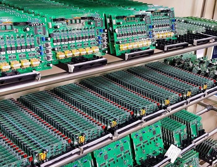
SMT assembly is the core link of GNSS electronics full-process manufacturing, determining product assembly precision and electrical performance. GNSS high-precision assembly adopts full-automatic SMT production line, strictly implementing standardized process steps including solder paste printing, high-precision placement, reflow soldering, and post-soldering inspection.
4.1 Solder Paste Printing Process
Solder paste printing is the foundation of high-quality soldering. GNSS production uses ultra-fine grain lead-free solder paste suitable for fine-pitch components. According to PCB pad design, a high-precision laser-cut stencil is customized to ensure uniform and consistent solder paste coating.
Printing parameters are precisely controlled: printing speed, pressure, and demoulding speed are adjusted according to component density and pad size to avoid insufficient solder, excessive solder, and solder paste deviation. After printing, 3D solder paste thickness detector is used to detect printing quality in real time, screening out unqualified PCB boards to ensure printing yield rate above 99.8%.
4.2 High-Precision Component Placement
GNSS modules contain a large number of miniature fine-pitch components, requiring high-precision placement equipment. The production line adopts high-speed and high-precision placement machines with placement accuracy up to ±0.025mm, which can accurately mount tiny components such as 0201 resistors and capacitors, fine-pitch RF chips, and ceramic antennas.
During placement, the system automatically identifies component polarity and PCB positioning marks to avoid reverse placement and offset errors. For key components such as antennas and connectors, secondary visual positioning is adopted to ensure accurate placement position, which effectively guarantees the integrity of RF signal transmission path and impedance matching effect.
4.3 Precision Reflow Soldering
Reflow soldering is a key process to realize permanent bonding between components and PCB. GNSS electronics adopt multi-zone convection reflow oven, with strictly optimized temperature profile to adapt to the characteristics of RF components and PCB substrates.
The standard reflow temperature profile is divided into four stages: preheating stage (160–180℃, 60–120s) to evaporate solder paste solvent and activate flux; heating-up stage with a heating rate controlled at 3℃/s to avoid rapid temperature rise causing component thermal damage; peak soldering stage (peak temperature 245℃, holding 10–30s) to ensure full solder melting and wetting; slow cooling stage with a cooling rate of 3℃/s to enhance solder joint strength and avoid solder joint cracking.
Precise temperature control effectively solves common soldering defects such as tombstoning, solder balls, cold solder, and voids, ensuring firm and consistent solder joints of GNSS precision components.
4.4 Post-Soldering AOI Visual Inspection
After reflow soldering, all products pass through Automated Optical Inspection (AOI) equipment for full inspection. AOI system uses high-definition camera and intelligent algorithm to automatically identify various assembly defects including missing components, wrong parts, polarity reversal, solder bridging, insufficient solder, and offset placement.
Compared with manual inspection, AOI full inspection realizes 100% coverage of product appearance defects, effectively avoiding missing inspection of tiny defects. Defective products are automatically marked and sent to rework station for targeted repair, ensuring all assembled PCBA boards meet appearance and assembly precision standards.
5. Functional Calibration and Professional Testing Process
Testing and calibration are the core links to verify GNSS product performance. Different from ordinary electronic product testing, GNSS electronics focus on RF signal performance, positioning accuracy, and environmental reliability. The full testing process includes functional testing, signal performance calibration, environmental reliability testing, and aging testing.
5.1 Basic Electrical Functional Testing
Basic electrical testing is carried out first to verify the basic working performance of the product, including power-on test, current and voltage test, circuit connectivity test, and communication function test. The test ensures that the product has no short circuit, open circuit, and power failure faults, and the serial port communication, data transmission, and other basic functions work normally, laying a foundation for subsequent professional positioning performance testing.
5.2 GNSS Signal Performance Calibration and Testing
Signal performance testing is the core of GNSS product testing, completed in a professional shielded test chamber to avoid external electromagnetic signal interference. Core test items include satellite signal sensitivity, positioning accuracy, TTFF, satellite tracking quantity, and signal stability.
Sensitivity testing verifies the product's ability to capture weak satellite signals, determining the positioning performance in sheltered environments such as indoors, urban canyons, and dense forests. TTFF testing counts the startup positioning time of cold start, warm start, and hot start to evaluate product response speed. Positioning accuracy testing adopts professional satellite signal simulation equipment to test static and dynamic positioning errors, ensuring that the error meets consumer-level, industrial-level, or surveying-level standards.
In addition, anti-interference testing is carried out to simulate complex electromagnetic environments, verify the product's signal anti-crosstalk ability, and ensure stable positioning in vehicle, industrial, and drone working scenarios.
5.3 Environmental Reliability Testing
To ensure the adaptability of GNSS electronics in complex working environments, batch sampling is carried out for environmental reliability testing, including high and low temperature cycling test, high temperature aging test, humidity resistance test, vibration test, and drop test.
The high and low temperature test adopts -40℃ to 85℃ cyclic temperature change to verify product performance stability in extreme temperature environments. The vibration and drop test simulates the vibration and impact during product transportation and operation, ensuring firm component assembly and no performance failure. The humidity resistance test verifies the product's waterproof and moisture-proof performance to adapt to outdoor and industrial humid environments.
5.4 Long-Term Aging Testing
Finished GNSS products undergo 72-hour continuous power-on aging testing. During the aging process, the system continuously records product positioning data, power consumption changes, and signal stability. Products with positioning drift, signal disconnection, and abnormal power consumption are screened out to ensure that the products delivered from the factory have long-term stable operational performance and no latent faults.
6. Post-Production Processing, Packaging and Quality Inspection
After testing and calibration are completed, GNSS electronics enter post-production processing, final quality inspection, and packaging links. Standardized post-processing ensures product consistency, integrity, and transportation safety.
6.1 Post-Production Fine Processing
Post-production processing includes laser marking, accessory assembly, and surface cleaning. Laser marking permanently prints product model, batch number, IMEI code, and production date on the product surface, which is convenient for product traceability and after-sales management. For integrated GNSS equipment, complete assembly of antennas, shells, and interfaces is carried out, and the whole machine is cleaned to remove surface dust and solder residues to ensure product appearance quality.
6.2 Final Quality Control (FQC)
FQC full inspection is implemented before product delivery. Inspectors conduct secondary verification of product appearance, assembly precision, functional performance, and test data. All products must meet batch consistency standards, with no appearance defects, stable positioning performance, and complete test data records. Unqualified products are reworked or scrapped in batches to ensure 100% factory qualification rate.
6.3 Professional Anti-Static Packaging and Warehousing
Qualified finished products adopt professional anti-static, moisture-proof, and shockproof packaging. Independent anti-static bags are used for single products, and foam shockproof materials are added for batch packaging to avoid product damage caused by static electricity, moisture, and vibration during transportation and storage. After packaging, products are stored in a constant temperature and humidity warehouse, and batch management is implemented to facilitate subsequent delivery and after-sales traceability.
7. Core Quality Control Standards and Industry Specifications
The full-process manufacturing of GNSS electronics strictly follows international and industry quality standards to ensure product professionalism and reliability. The core compliance standards include ISO9001 quality management system, IPC electronic assembly standards, and automotive-grade AEC-Q100 certification standards.
In the assembly process, IPC-A-610 electronic assembly appearance quality standards are strictly implemented to standardize solder joint quality, component placement, and product appearance. For automotive and industrial GNSS products, AEC-Q100 temperature resistance and reliability standards are met to ensure stable operation in harsh environments. All production links adopt standardized process documents and operation specifications, realizing whole-process traceability from raw material incoming, production processing, testing calibration to finished product delivery.
8. Application Fields and Manufacturing Customization Requirements
With the rapid development of intelligent positioning technology, GNSS electronics are widely used in multiple fields, and different application scenarios have customized manufacturing requirements for GNSS products.
Consumer-grade GNSS products (smart wearables, portable trackers) focus on miniaturization, low power consumption, and cost control. The manufacturing process optimizes component layout to reduce product volume, adopts low-power process calibration, and ensures stable basic positioning performance.
Industrial-grade GNSS products (drone positioning, industrial IoT monitoring) focus on high stability and anti-interference ability. The manufacturing process strengthens RF shielding design, environmental aging testing, and vibration resistance processing to adapt to complex industrial working environments.
Automotive-grade GNSS products (vehicle navigation, automatic driving positioning) meet AEC-Q100 certification standards, with stricter high and low temperature resistance, vibration resistance, and long-term reliability requirements in the manufacturing process.
High-precision surveying and mapping GNSS products (RTK positioning equipment) focus on ultra-high positioning accuracy. The manufacturing process optimizes impedance matching, clock calibration, and signal filtering technology, with more precise testing and calibration standards to achieve centimeter-level positioning accuracy.
GNSS electronics full process manufacturing is a systematic and precise engineering system covering design, procurement, assembly, testing, and packaging. Every link directly affects the final positioning accuracy, signal stability, and service life of GNSS products. With the continuous upgrading of intelligent positioning scenarios, the market has higher and higher requirements for GNSS product precision and reliability. Standardized, refined, and intelligent full-process manufacturing management has become the core competitiveness of GNSS electronic manufacturing enterprises.
Professional GNSS manufacturing strictly controls every production detail through standardized design optimization, high-precision SMT assembly, professional performance calibration, and strict quality inspection, providing high-reliability positioning hardware support for drones, autonomous driving, intelligent IoT, surveying and mapping, and aerospace fields. In the future, with the popularization of multi-system fusion positioning and high-precision RTK technology, GNSS electronics manufacturing will further develop towards miniaturization, high precision, low power consumption, and high reliability.
Lucy Yang | lucy.y@toxutech.com
Dotty Zhao | sales04@toxutech.com
Global Business Director / Sales Team / Global Operations


 En
 Cn
 Korean
 Home >
